

Signal Integrity vs Signal Delay
MAR 26, 20269 MIN READ
Generate Your Research Report Instantly with AI Agent
PatSnap Eureka helps you evaluate technical feasibility & market potential.
Signal Integrity and Delay Background and Objectives
Signal integrity and signal delay represent two fundamental yet interconnected challenges in modern electronic system design, particularly as digital circuits operate at increasingly higher frequencies and smaller geometries. Signal integrity encompasses the quality and fidelity of electrical signals as they propagate through transmission lines, connectors, and circuit board traces, while signal delay refers to the time required for signals to travel from source to destination within electronic systems.
The evolution of these challenges traces back to the early days of digital electronics when operating frequencies were relatively low and signal integrity concerns were minimal. However, as processor speeds increased from megahertz to gigahertz ranges and beyond, the wavelengths of digital signals became comparable to the physical dimensions of circuit board traces and interconnects. This fundamental shift transformed what were once simple electrical connections into complex transmission line structures requiring careful electromagnetic analysis.
The relationship between signal integrity and delay has become increasingly critical as modern electronic systems demand both high-speed operation and reliable signal transmission. Signal integrity degradation manifests through various phenomena including reflections, crosstalk, ground bounce, and power supply noise, all of which can introduce timing uncertainties and affect signal delay characteristics. Conversely, efforts to minimize signal delay through aggressive routing and high-speed design techniques can inadvertently compromise signal integrity if not properly managed.
Current technological trends driving these challenges include the proliferation of high-speed serial interfaces, multi-gigabit data rates, advanced packaging technologies, and the integration of mixed-signal circuits on single substrates. The semiconductor industry's continued pursuit of Moore's Law scaling, combined with the growing complexity of system-on-chip designs, has intensified the need for sophisticated signal integrity and timing analysis methodologies.
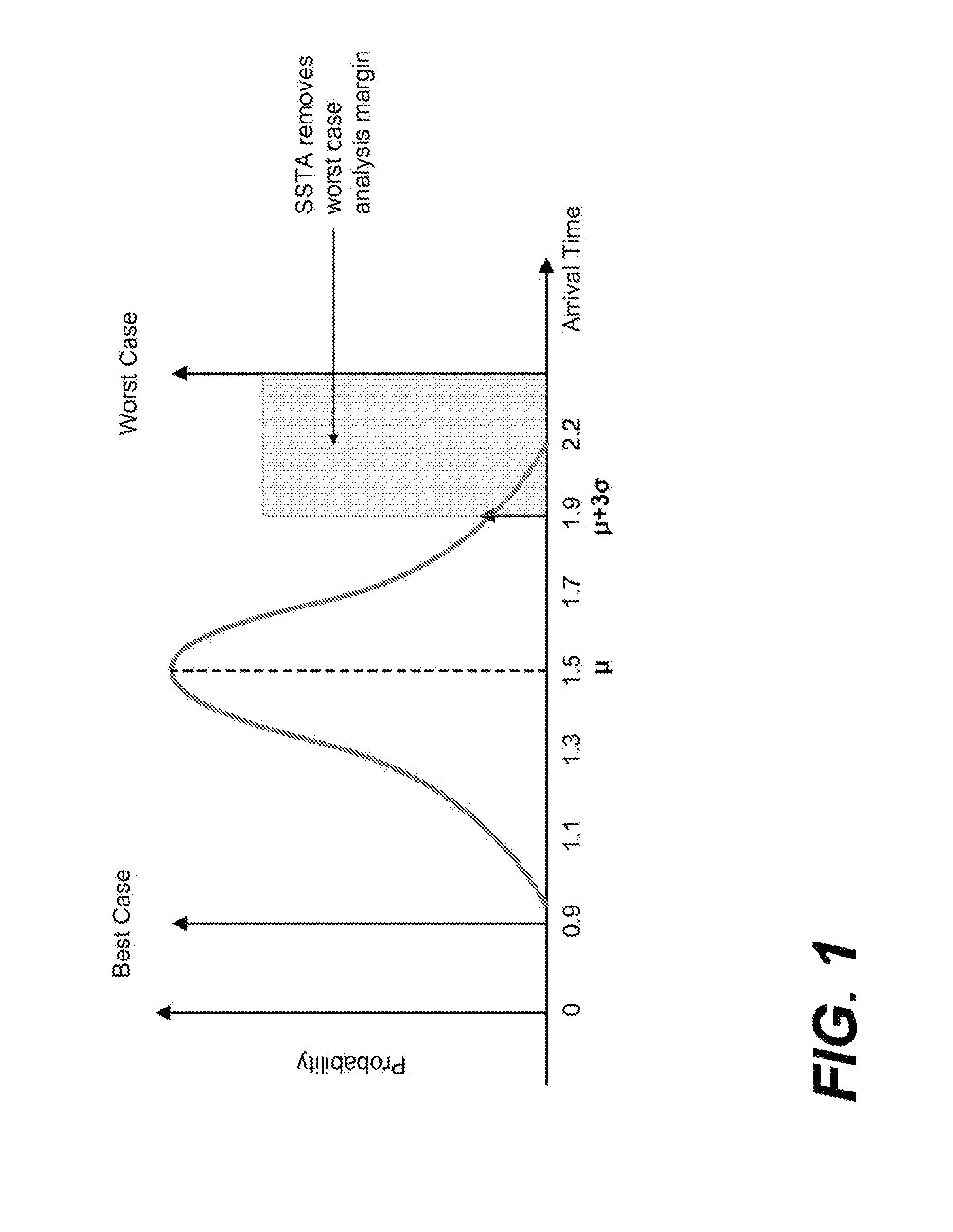
The primary objective in addressing signal integrity versus signal delay challenges is to achieve optimal balance between signal quality and timing performance while maintaining system reliability and cost-effectiveness. This involves developing comprehensive design methodologies that can simultaneously optimize both parameters, creating robust simulation and measurement techniques for accurate prediction and validation, and establishing design guidelines that enable engineers to make informed trade-offs between signal integrity and delay requirements based on specific application needs and performance targets.
The evolution of these challenges traces back to the early days of digital electronics when operating frequencies were relatively low and signal integrity concerns were minimal. However, as processor speeds increased from megahertz to gigahertz ranges and beyond, the wavelengths of digital signals became comparable to the physical dimensions of circuit board traces and interconnects. This fundamental shift transformed what were once simple electrical connections into complex transmission line structures requiring careful electromagnetic analysis.
The relationship between signal integrity and delay has become increasingly critical as modern electronic systems demand both high-speed operation and reliable signal transmission. Signal integrity degradation manifests through various phenomena including reflections, crosstalk, ground bounce, and power supply noise, all of which can introduce timing uncertainties and affect signal delay characteristics. Conversely, efforts to minimize signal delay through aggressive routing and high-speed design techniques can inadvertently compromise signal integrity if not properly managed.
Current technological trends driving these challenges include the proliferation of high-speed serial interfaces, multi-gigabit data rates, advanced packaging technologies, and the integration of mixed-signal circuits on single substrates. The semiconductor industry's continued pursuit of Moore's Law scaling, combined with the growing complexity of system-on-chip designs, has intensified the need for sophisticated signal integrity and timing analysis methodologies.
The primary objective in addressing signal integrity versus signal delay challenges is to achieve optimal balance between signal quality and timing performance while maintaining system reliability and cost-effectiveness. This involves developing comprehensive design methodologies that can simultaneously optimize both parameters, creating robust simulation and measurement techniques for accurate prediction and validation, and establishing design guidelines that enable engineers to make informed trade-offs between signal integrity and delay requirements based on specific application needs and performance targets.
Market Demand for High-Speed Signal Solutions
The global electronics industry is experiencing unprecedented demand for high-speed signal solutions as digital transformation accelerates across multiple sectors. Data centers, telecommunications infrastructure, automotive electronics, and consumer devices are driving this surge, with each sector presenting unique requirements for signal integrity and delay optimization. The proliferation of cloud computing, artificial intelligence workloads, and edge computing applications has created an insatiable appetite for faster data processing and transmission capabilities.
Telecommunications networks are undergoing massive upgrades to support 5G deployment and prepare for future 6G technologies. These next-generation networks require signal processing solutions that can handle extremely high frequencies while maintaining signal quality across complex transmission paths. The challenge extends beyond raw speed to encompass reliability, power efficiency, and miniaturization demands that push current technology boundaries.
The automotive sector represents a rapidly expanding market segment for high-speed signal solutions. Advanced driver assistance systems, autonomous vehicle technologies, and in-vehicle infotainment systems generate enormous data volumes that must be processed in real-time. Safety-critical applications in automotive electronics demand signal solutions that can guarantee both speed and reliability under harsh environmental conditions.
Consumer electronics continue to drive innovation in high-speed signal processing, particularly in smartphones, gaming devices, and high-resolution display technologies. The transition to higher refresh rates, increased pixel densities, and enhanced multimedia capabilities requires sophisticated signal management solutions that can deliver superior performance within increasingly compact form factors.
Enterprise computing and data center applications represent the largest market segment for high-speed signal solutions. The exponential growth in data generation, storage, and processing requirements has created demand for interconnect solutions that can support ever-increasing bandwidth requirements while minimizing latency and power consumption.
Emerging technologies such as quantum computing, neuromorphic processors, and advanced AI accelerators are creating new market opportunities for specialized high-speed signal solutions. These applications often require custom approaches to signal integrity and delay management that go beyond conventional design paradigms.
The market demand is further intensified by the ongoing trend toward system integration and miniaturization. Modern electronic systems must pack more functionality into smaller spaces while maintaining or improving performance levels, creating complex engineering challenges that drive innovation in signal processing technologies.
Current SI vs Delay Challenges and Constraints
The fundamental challenge in modern electronic systems lies in the inherent trade-off between signal integrity and signal delay optimization. As data rates continue to escalate beyond 100 Gbps in high-performance applications, engineers face increasingly complex constraints that prevent simultaneous achievement of optimal signal quality and minimal propagation delay.
Power delivery network limitations represent a critical constraint affecting both signal integrity and delay performance. Insufficient power supply decoupling creates voltage fluctuations that degrade signal quality while simultaneously forcing designers to implement conservative timing margins. The resulting power-ground bounce phenomena can introduce jitter exceeding 10 picoseconds in high-speed digital systems, directly impacting both signal fidelity and timing closure.
Crosstalk mitigation strategies inherently conflict with delay optimization objectives. Traditional approaches such as increased trace spacing and guard traces effectively reduce electromagnetic coupling but significantly extend signal path lengths. This spatial trade-off becomes particularly pronounced in dense packaging environments where routing constraints force designers to choose between acceptable crosstalk levels and meeting stringent timing requirements.
Manufacturing process variations introduce statistical uncertainties that compound SI-delay optimization challenges. Dielectric constant variations of ±5% in printed circuit board materials directly affect both characteristic impedance matching and propagation velocity. These variations force designers to implement worst-case design margins that sacrifice optimal performance in favor of yield reliability.
Thermal management constraints create additional complexity in balancing signal integrity against delay requirements. High-frequency signals generate significant heat in lossy transmission media, necessitating thermal mitigation strategies that often involve material selections with suboptimal electrical properties. The resulting compromise between thermal performance and electrical characteristics limits achievable signal quality and speed simultaneously.
Package and interconnect parasitics represent fundamental physical limitations that constrain both signal integrity and delay optimization. Bond wire inductances, via stubs, and package resonances create frequency-dependent impedance discontinuities that degrade signal quality while introducing unpredictable delay variations. These parasitic effects become increasingly dominant as signal rise times approach sub-100 picosecond ranges.
Current simulation and modeling tools exhibit limitations in accurately predicting the complex interactions between signal integrity and delay phenomena. Electromagnetic field solvers often require simplified models that may not capture the full complexity of real-world manufacturing variations and environmental conditions, leading to design margins that may be either insufficient or overly conservative.
Current Signal Integrity Design Solutions
01 Signal transmission line design and impedance matching
Proper design of signal transmission lines with controlled impedance is crucial for maintaining signal integrity. Techniques include optimizing trace width, spacing, and layer stackup in printed circuit boards. Impedance matching between transmission lines and termination points helps minimize signal reflections and distortions. Careful consideration of characteristic impedance and termination schemes ensures reliable signal propagation with minimal degradation.- Signal transmission line design and impedance matching: Proper design of signal transmission lines with controlled impedance is crucial for maintaining signal integrity. Techniques include optimizing trace width, spacing, and layer stackup in printed circuit boards. Impedance matching between transmission lines and termination points helps minimize signal reflections and distortions. Careful consideration of characteristic impedance and termination schemes ensures reliable signal propagation with minimal degradation.
- Delay compensation and timing adjustment circuits: Circuits and methods for compensating signal delays are essential in high-speed digital systems. These include programmable delay elements, phase-locked loops, and delay-locked loops that can dynamically adjust timing to maintain synchronization. Techniques involve detecting timing mismatches and applying corrective delays to ensure proper signal alignment across multiple channels or clock domains.
- Crosstalk reduction and electromagnetic interference mitigation: Methods to reduce crosstalk between adjacent signal lines include increasing spacing between traces, using ground planes as shields, and implementing differential signaling. Electromagnetic interference can be minimized through proper grounding techniques, shielding, and filtering. These approaches help maintain signal integrity by preventing unwanted coupling and noise injection that can cause signal degradation and timing errors.
- Signal equalization and pre-emphasis techniques: Equalization techniques compensate for frequency-dependent losses in transmission channels by boosting high-frequency components. Pre-emphasis involves intentionally distorting the transmitted signal to counteract known channel characteristics. These methods help restore signal quality at the receiver by compensating for attenuation and dispersion effects that occur during transmission, thereby improving overall signal integrity.
- Simulation and measurement tools for signal integrity analysis: Advanced simulation tools and measurement techniques enable engineers to analyze and predict signal integrity issues before physical implementation. These include time-domain reflectometry, vector network analysis, and electromagnetic field simulation software. Such tools help identify potential problems related to impedance discontinuities, reflections, and timing violations, allowing for design optimization to ensure reliable signal transmission.
02 Delay compensation and timing adjustment circuits
Circuits and methods for compensating signal delays are essential in high-speed digital systems. These include programmable delay elements, phase-locked loops, and delay-locked loops that can dynamically adjust signal timing. Techniques involve measuring propagation delays and applying corrective adjustments to synchronize signals across different paths. Such compensation mechanisms ensure proper timing relationships between clock and data signals in complex integrated circuits.Expand Specific Solutions03 Crosstalk reduction and electromagnetic interference mitigation
Minimizing crosstalk between adjacent signal lines is critical for preserving signal integrity. Techniques include increasing spacing between traces, using ground planes as shields, and implementing differential signaling. Proper grounding and shielding strategies help reduce electromagnetic interference from external sources. Layout optimization and the use of guard traces can effectively isolate sensitive signals from noise sources.Expand Specific Solutions04 Signal equalization and pre-emphasis techniques
Equalization methods compensate for frequency-dependent losses in transmission channels. Pre-emphasis techniques boost high-frequency components of signals before transmission to counteract attenuation. Adaptive equalization circuits can dynamically adjust to varying channel conditions. These techniques are particularly important in high-speed serial communication links where signal degradation over long distances can significantly impact data integrity.Expand Specific Solutions05 Jitter analysis and clock distribution networks
Jitter, representing timing variations in signals, directly affects signal integrity and system performance. Analysis techniques identify sources of deterministic and random jitter in clock and data signals. Clock distribution networks must be carefully designed to minimize skew and jitter across multiple destinations. Buffering strategies, tree structures, and phase-locked loops help maintain consistent timing throughout large integrated circuits and systems.Expand Specific Solutions
Key Players in SI and High-Speed Design Industry
The signal integrity versus signal delay technology landscape represents a mature yet rapidly evolving sector driven by increasing demands for high-speed digital communications and advanced semiconductor applications. The market demonstrates substantial growth potential, particularly in 5G, automotive, and high-performance computing segments. Technology maturity varies significantly across players, with established leaders like Synopsys, Cadence Design Systems, and Rambus offering sophisticated EDA tools and interface technologies for signal integrity optimization. Semiconductor giants including AMD, MediaTek, and Realtek integrate advanced signal management solutions into their chip designs, while infrastructure providers like Huawei, Ericsson, and NEC implement these technologies in telecommunications equipment. Manufacturing leaders such as GlobalFoundries and Hon Hai Precision ensure signal integrity in production processes, indicating a comprehensive ecosystem spanning design, manufacturing, and implementation phases across multiple industry verticals.
Huawei Technologies Co., Ltd.
Technical Solution: Huawei has developed comprehensive signal integrity solutions for high-speed digital systems, focusing on advanced PCB design methodologies and signal routing optimization. Their approach includes differential pair routing techniques, controlled impedance design, and crosstalk mitigation strategies. The company implements sophisticated simulation tools for pre-layout signal integrity analysis and employs advanced materials with low dielectric constants to minimize signal delay. Their solutions particularly excel in 5G infrastructure equipment where maintaining signal quality while minimizing latency is critical for network performance.
Strengths: Strong expertise in high-frequency design and 5G applications. Weaknesses: Limited availability of detailed technical documentation due to trade restrictions.
Apple, Inc.
Technical Solution: Apple focuses on signal integrity optimization in mobile device design, implementing advanced packaging technologies and custom silicon solutions. Their approach emphasizes minimizing signal delay through optimized die-to-die interconnects and sophisticated power delivery networks. Apple's signal integrity strategy includes the use of advanced materials, precise impedance control, and innovative layout techniques to maintain signal quality in compact form factors. Their custom-designed processors incorporate on-chip signal conditioning and timing optimization to balance signal integrity with performance requirements in power-constrained environments.
Strengths: Excellent integration of hardware and software optimization, leading-edge packaging technology. Weaknesses: Proprietary solutions limit broader industry applicability.
Core SI-Delay Trade-off Innovations
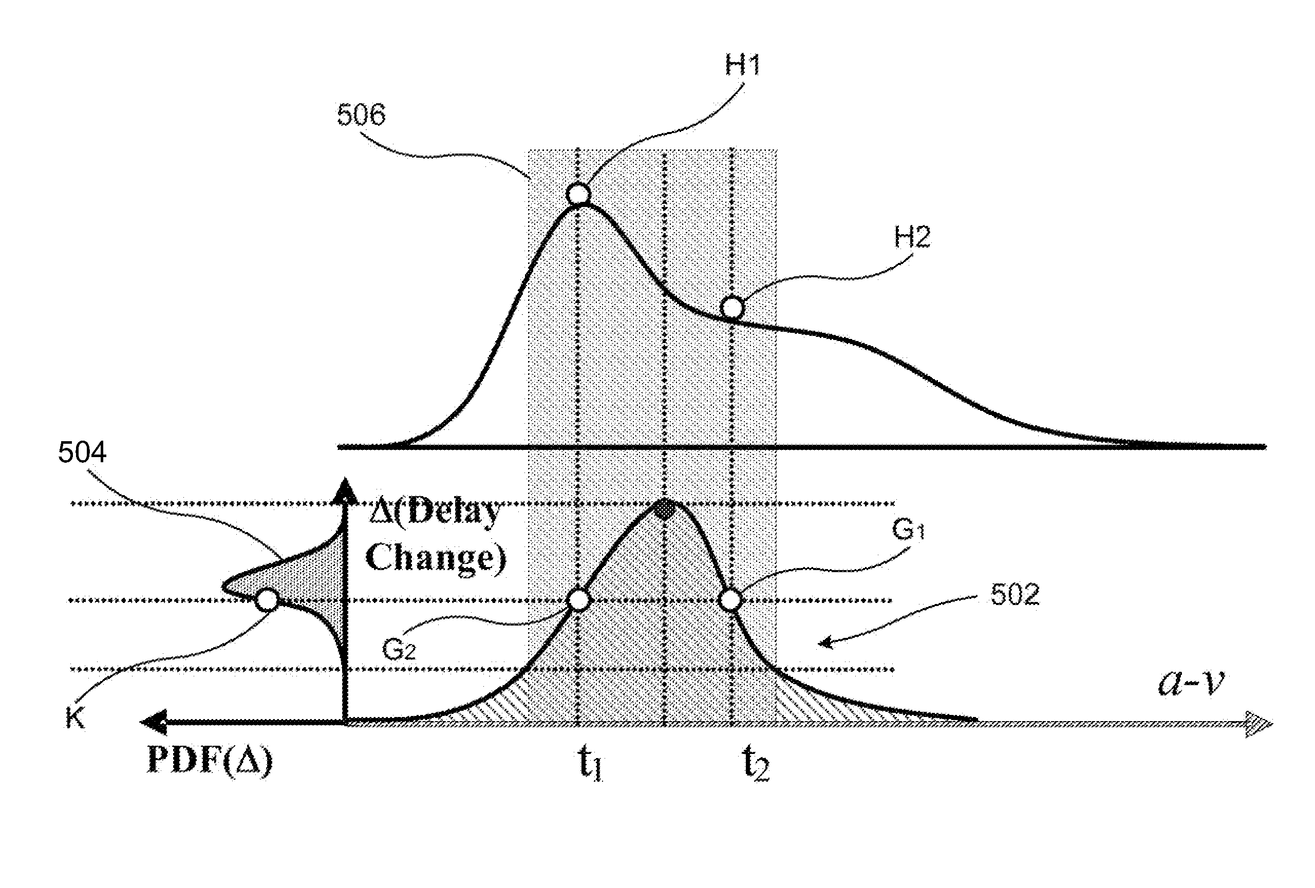
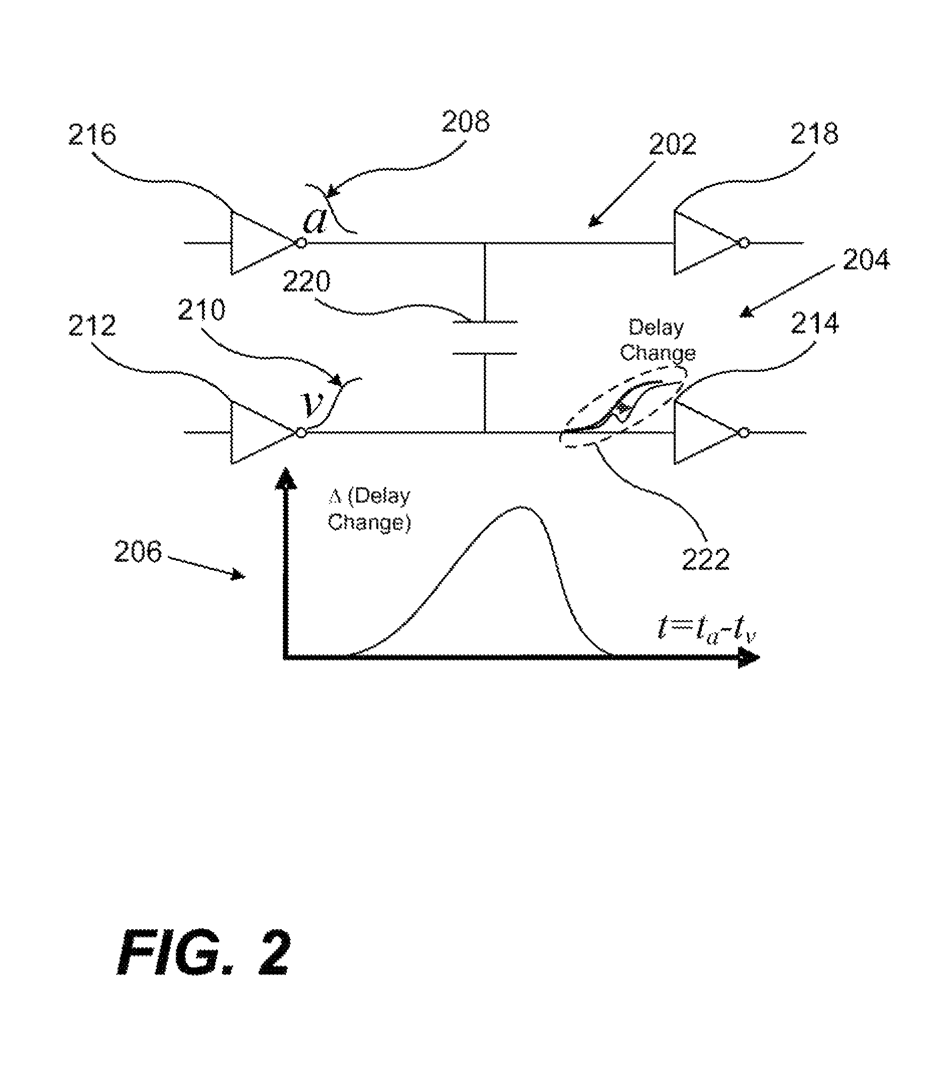
Statistical static timing analysis of signal with crosstalk induced delay change in integrated circuit
PatentInactiveUS8244491B1
Innovation
- The implementation of statistical static timing analysis (SSTA) to evaluate crosstalk-induced delay changes by generating separate probability density functions (PDFs) for aggressor switching and combining them to determine a delay change curve, which is then used to calculate the PDF of victim net signal transition time under crosstalk influence.

Delay and signal integrity check and characterization
PatentInactiveUS7203918B2
Innovation
- A method for performing signal integrity and delay checks in circuit simulations by selecting nodes, determining optimization parameters, and iteratively adjusting these parameters to achieve convergence, using bisection error calculations to identify and address switch difference and delay difference errors, thereby ensuring accurate characterization and optimization of setup and hold times.


EMC Compliance for Signal Integrity
Electromagnetic compatibility (EMC) compliance represents a critical regulatory framework that directly impacts signal integrity design and implementation across electronic systems. Modern electronic devices must satisfy stringent EMC standards such as FCC Part 15, CISPR 22, and EN 55032, which establish limits for both conducted and radiated emissions while defining immunity requirements against external electromagnetic interference.
Signal integrity engineers must navigate complex EMC requirements that often conflict with optimal electrical performance objectives. High-speed digital signals inherently generate broadband electromagnetic emissions, particularly at fundamental frequencies and harmonics where switching transitions create spectral content extending well into gigahertz ranges. These emissions must be controlled through careful PCB layout techniques, including proper ground plane design, controlled impedance routing, and strategic component placement.
Compliance testing reveals that signal integrity violations frequently manifest as EMC failures during pre-compliance and formal certification processes. Common failure modes include excessive radiated emissions from poorly terminated transmission lines, ground bounce effects creating common-mode currents, and inadequate filtering of power distribution networks. These issues necessitate iterative design modifications that can significantly impact project timelines and development costs.
Regulatory standards impose specific measurement methodologies using standardized test equipment and environments, such as anechoic chambers for radiated emissions testing and line impedance stabilization networks (LISN) for conducted emissions evaluation. Understanding these test procedures enables proactive design strategies that anticipate measurement conditions and potential failure mechanisms during the design phase rather than post-prototype testing.
The integration of EMC compliance considerations into signal integrity design workflows requires sophisticated simulation tools capable of predicting electromagnetic field distributions and coupling mechanisms. Advanced electromagnetic solvers can model complex PCB geometries and predict potential compliance issues before physical prototyping, enabling design optimization that simultaneously addresses signal quality and regulatory requirements while minimizing the risk of costly redesign cycles.
Power Integrity Impact on Signal Performance
Power integrity fundamentally influences signal performance through multiple interconnected mechanisms that directly affect both signal quality and timing characteristics. The power distribution network serves as the foundation for all digital operations, where voltage fluctuations and noise propagation create cascading effects throughout the entire system architecture.
Voltage droop represents one of the most critical power integrity challenges affecting signal performance. When instantaneous current demands exceed the power delivery network's capability, supply voltages temporarily decrease below nominal levels. This phenomenon directly impacts driver strength and switching thresholds, leading to degraded signal rise and fall times. Consequently, timing margins become compressed, and signal integrity parameters such as eye diagram openings deteriorate significantly.
Ground bounce and simultaneous switching noise constitute another major pathway through which power integrity affects signal behavior. Multiple drivers switching concurrently create substantial current transients through shared power and ground connections. These transients manifest as voltage variations across the reference planes, effectively modulating the signal paths and introducing timing uncertainties that compound traditional signal delay variations.
Power supply noise coupling mechanisms create additional signal performance degradation through substrate and package-level interactions. High-frequency noise components present in power rails couple into sensitive signal paths through parasitic capacitances and inductive coupling. This coupling introduces jitter components that directly correlate with power integrity metrics, creating a measurable relationship between supply noise characteristics and signal timing performance.
The impedance characteristics of power distribution networks significantly influence signal return path integrity, particularly in high-speed digital systems. Inadequate decoupling or resonant behavior in power delivery structures creates impedance discontinuities that affect signal return currents. These discontinuities translate into signal integrity issues including reflections, crosstalk enhancement, and timing skew between differential pairs.
Modern system designs must consider power integrity as an integral component of signal performance optimization rather than treating these domains independently. Advanced modeling techniques now incorporate power network impedance profiles into signal integrity simulations, enabling more accurate prediction of system-level performance under realistic operating conditions.
Unlock deeper insights with PatSnap Eureka Quick Research — get a full tech report to explore trends and direct your research. Try now!
Generate Your Research Report Instantly with AI Agent
Supercharge your innovation with PatSnap Eureka AI Agent Platform!