

Signal Integrity vs High-Speed Interfaces
MAR 26, 20269 MIN READ
Generate Your Research Report Instantly with AI Agent
PatSnap Eureka helps you evaluate technical feasibility & market potential.
Signal Integrity Challenges in High-Speed Interface Evolution
Signal integrity has emerged as one of the most critical challenges in modern high-speed interface design, fundamentally reshaping how engineers approach system architecture and implementation. As data transmission rates continue to escalate from gigabit to terabit speeds, the traditional boundaries between digital and analog design have become increasingly blurred, demanding a comprehensive understanding of electromagnetic phenomena that were once considered negligible.
The evolution of high-speed interfaces has introduced unprecedented complexity in maintaining signal fidelity across various transmission mediums. Contemporary systems operating at multi-gigahertz frequencies face severe degradation mechanisms including crosstalk, reflection, attenuation, and jitter, which collectively threaten data integrity and system reliability. These challenges are particularly pronounced in dense packaging environments where multiple high-speed channels operate in close proximity.
Power delivery network integrity has become inextricably linked with signal integrity performance, as simultaneous switching noise and power supply variations directly impact signal quality. The increasing current demands of high-performance processors and the shrinking voltage margins have created a complex interdependency between power and signal domains that requires holistic design approaches.
Electromagnetic interference and compatibility considerations have evolved from secondary concerns to primary design constraints. The proliferation of wireless communication standards and the increasing sensitivity of high-speed circuits to external interference have necessitated sophisticated shielding strategies and careful frequency planning to ensure coexistence of multiple systems within confined spaces.
Advanced packaging technologies, including 2.5D and 3D integration, have introduced novel signal integrity challenges related to through-silicon vias, interposer routing, and thermal management. These emerging architectures demand innovative modeling techniques and design methodologies to predict and mitigate signal degradation effects that span multiple physical domains and frequency ranges.
The convergence of artificial intelligence workloads and high-performance computing has further intensified signal integrity requirements, as these applications demand both high bandwidth and ultra-low latency communication between processing elements, pushing the boundaries of what is achievable with conventional design approaches.
Market Demand for Advanced High-Speed Interface Solutions
The global demand for advanced high-speed interface solutions has experienced unprecedented growth driven by the exponential increase in data transmission requirements across multiple industries. Cloud computing infrastructure, artificial intelligence applications, and edge computing deployments are creating substantial pressure on existing interface technologies to deliver higher bandwidth while maintaining signal integrity. Data centers worldwide are transitioning from traditional copper-based interconnects to advanced optical and electrical solutions capable of supporting multi-gigabit and terabit-scale communications.
Consumer electronics markets are simultaneously driving demand for enhanced interface performance, particularly in gaming, virtual reality, and high-resolution display applications. The proliferation of 8K displays, augmented reality devices, and real-time streaming services requires interface solutions that can handle massive data throughput without compromising signal quality. Mobile device manufacturers are increasingly adopting advanced interface standards to support faster charging, high-speed data transfer, and seamless connectivity across multiple protocols.
Automotive industry transformation toward autonomous vehicles and electric platforms has created new market segments for high-speed interface solutions. Advanced driver assistance systems, in-vehicle networking, and battery management systems demand robust interface technologies that can operate reliably in harsh electromagnetic environments while maintaining strict timing requirements. The integration of multiple sensors, cameras, and processing units within modern vehicles necessitates sophisticated interface architectures capable of handling diverse data streams simultaneously.
Telecommunications infrastructure modernization, particularly the global rollout of 5G networks and preparation for 6G technologies, represents a significant market driver for advanced interface solutions. Network equipment manufacturers require interface technologies that can support the increased bandwidth demands of next-generation wireless systems while addressing the complex signal integrity challenges associated with higher frequency operations.
Industrial automation and Internet of Things deployments are expanding market opportunities for specialized high-speed interface solutions. Manufacturing systems increasingly rely on real-time data exchange between sensors, controllers, and processing units, creating demand for interface technologies that can deliver deterministic performance in electrically noisy industrial environments. The convergence of operational technology and information technology systems requires interface solutions that can bridge traditional industrial protocols with modern high-speed communication standards.
Current SI Issues and Limitations in High-Speed Design
High-speed digital systems face increasingly complex signal integrity challenges as data rates continue to escalate beyond 100 Gbps in modern applications. Traditional design methodologies struggle to maintain signal quality when dealing with sub-picosecond rise times and multi-gigahertz switching frequencies. The fundamental physics of electromagnetic wave propagation becomes the dominant factor, making classical lumped-element circuit analysis inadequate for accurate system characterization.
Crosstalk represents one of the most persistent challenges in contemporary high-speed designs. As trace densities increase to accommodate more functionality in smaller form factors, electromagnetic coupling between adjacent conductors intensifies significantly. Near-end crosstalk (NEXT) and far-end crosstalk (FEXT) can corrupt data signals, leading to increased bit error rates and system performance degradation. Current mitigation techniques, including guard traces and differential signaling, provide limited effectiveness at frequencies exceeding 50 GHz.
Power delivery network (PDN) integrity poses another critical limitation in high-speed interface design. Modern processors and high-speed transceivers demand instantaneous current with minimal voltage ripple, yet traditional decoupling strategies fail to address the broadband noise spectrum generated by switching activities. The impedance profile of PDNs exhibits resonant peaks that can amplify noise at specific frequencies, creating voltage fluctuations that directly impact signal timing and amplitude integrity.
Interconnect losses become increasingly problematic as signal frequencies approach the multi-gigahertz range. Dielectric losses in PCB materials and conductor losses due to skin effect and surface roughness significantly attenuate high-frequency signal components. These frequency-dependent losses cause signal distortion, inter-symbol interference, and reduced eye diagram margins. Current equalization techniques, while helpful, introduce additional complexity and power consumption without fully addressing the underlying physical limitations.
Package and connector discontinuities create reflection and resonance issues that severely impact signal quality in high-speed systems. Via transitions, bond wire inductances, and impedance mismatches generate unwanted reflections that can cause signal integrity violations. The electrical length of these discontinuities becomes significant relative to signal wavelengths, making their effects more pronounced and difficult to compensate through traditional design approaches.
Thermal effects introduce additional complexity to signal integrity management in high-speed designs. Temperature variations affect material properties, causing impedance shifts and timing variations that can compromise system performance. The interaction between thermal management requirements and electrical performance optimization often creates conflicting design constraints that current methodologies struggle to resolve effectively.
Existing SI Mitigation Techniques for High-Speed Interfaces
01 Impedance matching and termination techniques
Signal integrity in high-speed interfaces can be improved through proper impedance matching and termination techniques. These methods help reduce signal reflections and maintain signal quality by matching the characteristic impedance of transmission lines with source and load impedances. Termination resistors and controlled impedance designs are employed to minimize signal distortion and ensure reliable data transmission at high frequencies.- Impedance matching and termination techniques: Signal integrity in high-speed interfaces can be improved through proper impedance matching and termination techniques. These methods help reduce signal reflections and maintain signal quality by matching the characteristic impedance of transmission lines with source and load impedances. Termination resistors and controlled impedance designs are employed to minimize signal distortion and ensure reliable data transmission at high frequencies.
- Differential signaling architectures: Differential signaling is widely used in high-speed interfaces to enhance signal integrity by transmitting data using paired signals with opposite polarity. This approach provides better noise immunity, reduces electromagnetic interference, and allows for higher data rates. The differential architecture helps cancel common-mode noise and improves signal-to-noise ratio, making it suitable for applications requiring robust high-speed data transmission.
- Equalization and pre-emphasis circuits: Equalization and pre-emphasis techniques are employed to compensate for signal degradation in high-speed interfaces. These circuits adjust signal amplitude and frequency characteristics to counteract losses caused by transmission media. Pre-emphasis boosts high-frequency components before transmission, while equalization restores signal integrity at the receiver end, enabling reliable communication over longer distances and at higher data rates.
- Clock and data recovery mechanisms: Clock and data recovery systems are essential for maintaining synchronization in high-speed interfaces. These mechanisms extract timing information from incoming data streams and regenerate clean clock signals for proper data sampling. Advanced phase-locked loops and clock recovery circuits ensure accurate data capture even in the presence of jitter and timing variations, which is critical for maintaining signal integrity in high-speed serial communications.
- PCB layout and routing optimization: Proper printed circuit board layout and routing strategies are crucial for maintaining signal integrity in high-speed interfaces. Techniques include controlled trace lengths, differential pair routing, ground plane design, and via optimization to minimize crosstalk, electromagnetic interference, and signal degradation. Careful attention to layer stackup, trace spacing, and return path continuity helps ensure reliable high-speed signal transmission across the board.
02 Differential signaling architectures
Differential signaling is widely used in high-speed interfaces to enhance signal integrity by transmitting data using paired signals with opposite polarity. This approach provides better noise immunity and reduces electromagnetic interference compared to single-ended signaling. The differential architecture helps maintain signal quality over longer distances and at higher data rates by canceling common-mode noise and improving signal-to-noise ratio.Expand Specific Solutions03 Pre-emphasis and equalization circuits
Pre-emphasis and equalization techniques are employed to compensate for signal degradation in high-speed transmission channels. These circuits boost high-frequency components of signals to counteract frequency-dependent losses and inter-symbol interference. Adaptive equalization algorithms can dynamically adjust signal characteristics to maintain optimal signal integrity across varying channel conditions and transmission distances.Expand Specific Solutions04 PCB layout and routing optimization
Proper printed circuit board layout and routing strategies are critical for maintaining signal integrity in high-speed interfaces. Techniques include controlled trace lengths, minimized via usage, appropriate layer stackup design, and careful consideration of ground planes. These design practices help reduce crosstalk, minimize electromagnetic interference, and maintain consistent signal propagation characteristics throughout the transmission path.Expand Specific Solutions05 Clock distribution and jitter reduction
Effective clock distribution networks and jitter reduction techniques are essential for high-speed interface performance. These solutions include phase-locked loops, clock buffers with low skew characteristics, and careful power supply filtering. Minimizing timing uncertainties and maintaining precise clock synchronization across multiple channels ensures reliable data sampling and reduces bit error rates in high-speed communication systems.Expand Specific Solutions
Key Players in High-Speed Interface and SI Solutions
The signal integrity versus high-speed interfaces technology landscape represents a mature yet rapidly evolving sector driven by increasing data transmission demands across computing, telecommunications, and consumer electronics. The market demonstrates substantial scale with established players like Intel, Samsung Electronics, and SK Hynix leading semiconductor innovations, while Rambus specializes in advanced memory architectures and interface technologies. Technology maturity varies significantly across segments, with companies like Tektronix and Advantest providing sophisticated testing solutions, while emerging players such as Nanjing Lanyang focus on AI-integrated applications. The competitive environment spans from traditional semiconductor giants (Huawei, MediaTek, Sony) to specialized connector manufacturers (Molex) and system integrators (Hon Hai, Inventec), indicating a fragmented but interconnected ecosystem where signal integrity solutions are increasingly critical for next-generation high-speed interface implementations across automotive, mobile, and data center applications.
Rambus, Inc.
Technical Solution: Rambus specializes in high-speed memory interface technologies with advanced signal integrity solutions including their proprietary differential signaling architectures, advanced equalization techniques, and innovative clocking schemes. Their technology portfolio encompasses DDR5/GDDR6 interface solutions, SerDes IP with built-in signal integrity optimization, and comprehensive PHY solutions that address power delivery, crosstalk mitigation, and timing closure challenges. Rambus implements sophisticated calibration algorithms and adaptive compensation mechanisms to maintain signal quality across process, voltage, and temperature variations in high-speed memory systems.
Strengths: Deep expertise in memory interface design, proven track record in high-speed signaling, strong IP portfolio and licensing model. Weaknesses: Limited to memory-focused applications, dependency on licensing revenue, less presence in general-purpose computing markets.
Intel Corp.
Technical Solution: Intel has developed comprehensive signal integrity solutions for high-speed interfaces including advanced package technologies, on-die termination schemes, and sophisticated equalization techniques. Their approach includes implementing adaptive equalization algorithms, crosstalk mitigation through optimized routing strategies, and power delivery network optimization to maintain signal quality at multi-gigabit data rates. Intel's solutions span from processor-level implementations to system-level design methodologies, incorporating machine learning-based signal integrity prediction and real-time compensation mechanisms for next-generation computing platforms.
Strengths: Industry-leading expertise in high-speed processor design, comprehensive ecosystem support, advanced manufacturing capabilities. Weaknesses: High complexity and cost, primarily focused on x86 architecture, limited flexibility for custom applications.
Core SI Innovations in High-Speed Interface Design
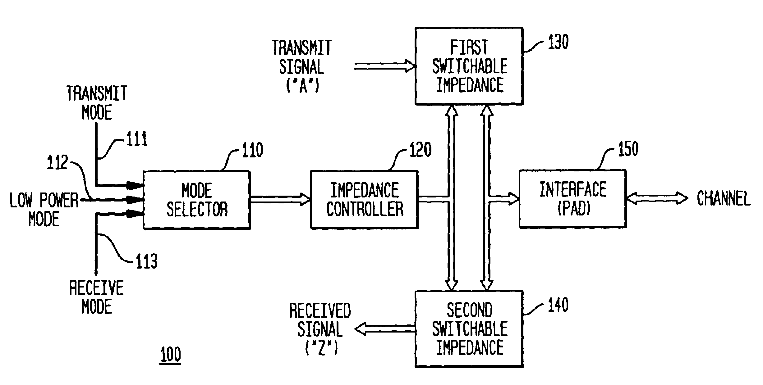
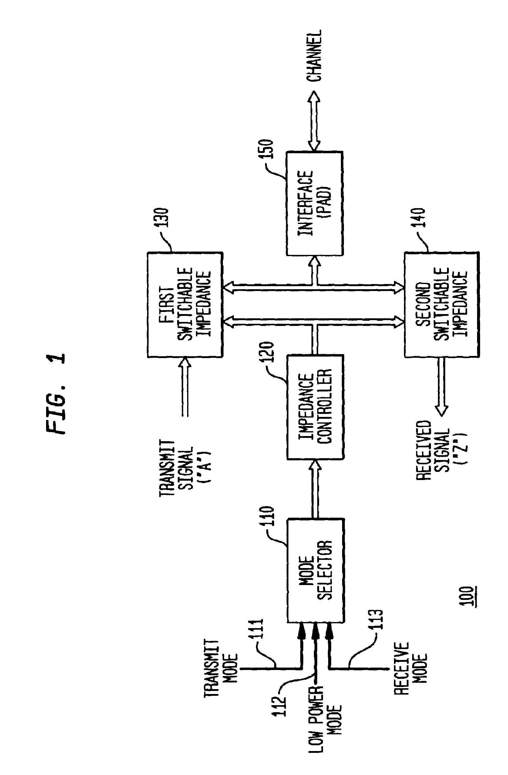
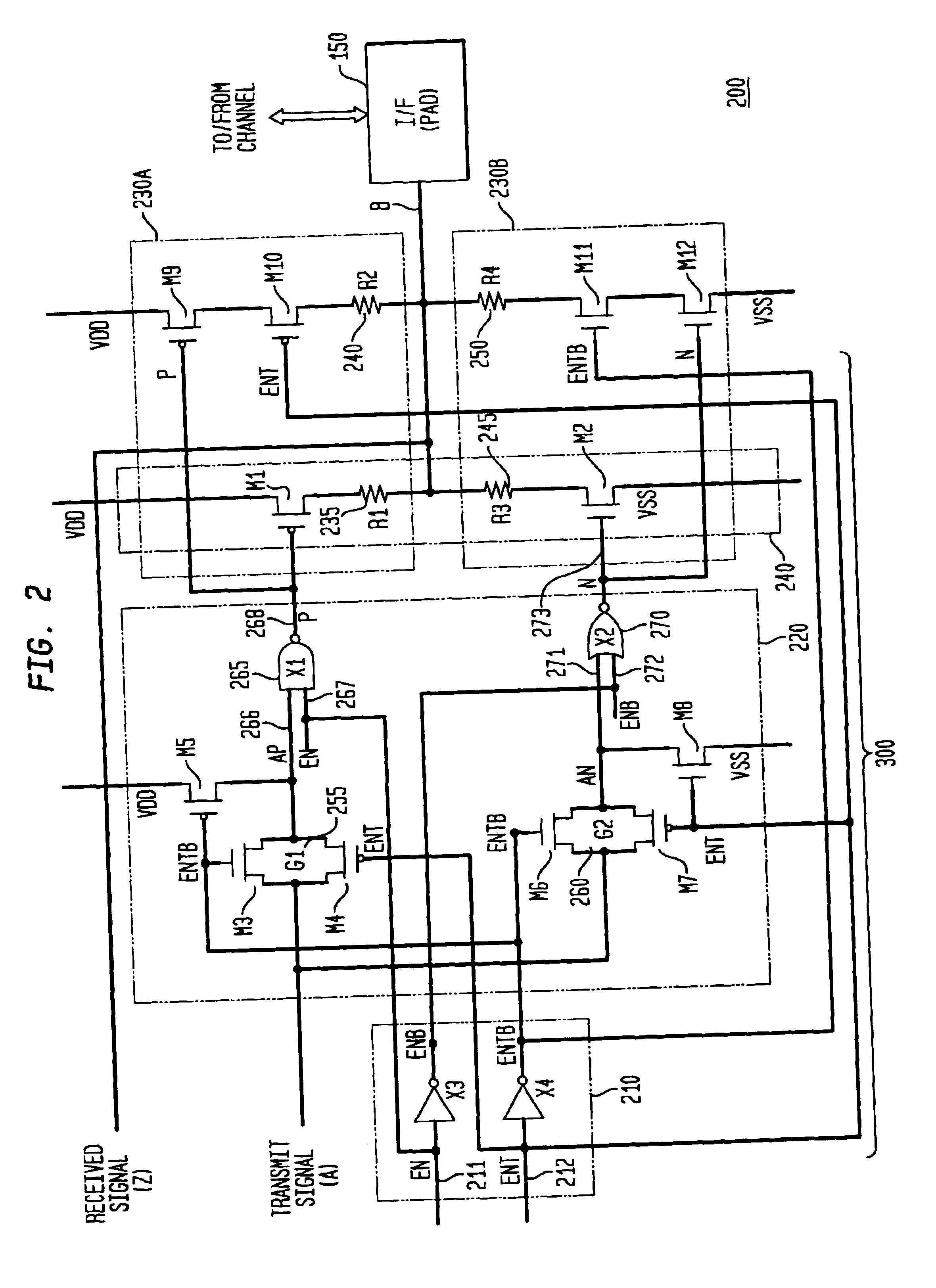
Bi-directional impedance matching circuit
PatentInactiveUS6850091B2
Innovation
- A bi-directional impedance matching apparatus with switchable impedances and an impedance controller that selectively matches output and input impedances to the channel impedance, including a mode selector for transmit, receive, and low power modes, eliminating the need for external resistors and reducing power dissipation.
Plug Standards-Compliant Circuit Modules and Connectors
PatentActiveUS20150163944A1
Innovation
- A circuit module design with a PCB configured to minimize impedance discontinuities, featuring tabs with coplanar conductive pads that match the dimensional requirements of standards-compliant receptacles, such as SFF 8639 or SATA specifications, reducing the need for separate connectors and integrating electrical contacts directly into the module housing.


Industry Standards and Compliance for High-Speed SI
The landscape of high-speed signal integrity is governed by a comprehensive framework of industry standards that ensure interoperability, performance consistency, and design reliability across diverse applications. These standards serve as critical benchmarks for engineers developing high-speed interfaces, providing essential guidelines for signal quality, timing parameters, and electrical characteristics.
IEEE standards form the backbone of high-speed interface specifications, with IEEE 802.3 defining Ethernet protocols from 1 Gbps to 400 Gbps and beyond. The standard establishes precise requirements for signal amplitude, rise times, jitter tolerance, and crosstalk limits. Similarly, IEEE 1596.3 addresses high-speed backplane applications, while IEEE P802.3ck focuses on emerging 800 Gbps Ethernet implementations, pushing the boundaries of current signal integrity capabilities.
JEDEC standards play a pivotal role in memory interface compliance, particularly for DDR4, DDR5, and emerging DDR6 technologies. These specifications define critical parameters including setup and hold times, voltage levels, and eye diagram requirements. The JEDEC JESD79 series establishes stringent signal integrity criteria that directly impact system performance and reliability in high-bandwidth memory applications.
PCI Express standards, managed by PCI-SIG, continue evolving with PCIe 5.0 and 6.0 specifications demanding increasingly sophisticated signal integrity solutions. These standards mandate specific equalization techniques, error correction mechanisms, and channel loss budgets that directly influence design methodologies and validation procedures.
Compliance verification requires advanced measurement techniques and specialized equipment capable of characterizing high-frequency behavior. Vector network analyzers, real-time oscilloscopes, and bit error rate testers must meet calibration standards traceable to national metrology institutes. The measurement uncertainty and repeatability requirements become increasingly stringent as data rates exceed 100 Gbps.
Regulatory compliance extends beyond performance specifications to encompass electromagnetic compatibility and safety requirements. FCC Part 15, CISPR standards, and regional EMC directives establish emission limits that significantly impact high-speed design strategies, often requiring careful balance between signal integrity optimization and electromagnetic interference mitigation.
SI Testing and Validation Methodologies
Signal integrity testing and validation methodologies have evolved into sophisticated frameworks that encompass both pre-silicon simulation and post-silicon measurement approaches. These methodologies are essential for ensuring high-speed interface performance meets stringent specifications while maintaining reliable data transmission across various operating conditions.
Pre-silicon validation relies heavily on electromagnetic simulation tools that model signal propagation through complex interconnect structures. Time-domain reflectometry simulations predict impedance discontinuities, while frequency-domain analysis identifies resonances and bandwidth limitations. Advanced modeling techniques incorporate statistical variations in manufacturing processes, enabling Monte Carlo analysis to assess yield implications and design robustness.
Post-silicon testing methodologies utilize specialized instrumentation including high-bandwidth oscilloscopes, vector network analyzers, and bit error rate testers. Eye diagram analysis remains fundamental for evaluating signal quality, measuring parameters such as eye height, eye width, and jitter characteristics. Complementary cumulative distribution function analysis provides statistical insights into timing margins and error probabilities.
Automated test equipment platforms have revolutionized validation efficiency by implementing standardized test suites that cover compliance testing for industry specifications like PCIe, USB, and DDR memory interfaces. These platforms integrate real-time signal processing capabilities, enabling on-the-fly correction and adaptive equalization assessment during validation campaigns.
Emerging validation approaches incorporate machine learning algorithms to predict signal integrity performance based on design parameters and measured characteristics. These methodologies enable rapid design space exploration and optimization, reducing traditional iterative design cycles. Additionally, in-system validation techniques using embedded test structures provide continuous monitoring capabilities for deployed systems.
The integration of correlation methodologies between simulation predictions and measurement results ensures validation accuracy and builds confidence in design methodologies. Statistical correlation analysis identifies systematic discrepancies, enabling continuous improvement of modeling accuracy and measurement techniques for future high-speed interface developments.
Unlock deeper insights with PatSnap Eureka Quick Research — get a full tech report to explore trends and direct your research. Try now!
Generate Your Research Report Instantly with AI Agent
Supercharge your innovation with PatSnap Eureka AI Agent Platform!