

Spintronics vs Traditional Memory: Access Time Comparison
APR 16, 20269 MIN READ
Generate Your Research Report Instantly with AI Agent
Patsnap Eureka helps you evaluate technical feasibility & market potential.
Spintronic Memory Technology Background and Objectives
Spintronic memory technology represents a paradigm shift in data storage, leveraging the intrinsic spin property of electrons alongside their charge to encode and process information. This revolutionary approach emerged from the fundamental understanding that electron spin can exist in two distinct states - up or down - providing a natural binary system for digital storage. Unlike conventional memory technologies that rely solely on electrical charge manipulation, spintronics harnesses quantum mechanical properties to achieve superior performance characteristics.
The historical development of spintronics traces back to the discovery of giant magnetoresistance (GMR) in the late 1980s, which demonstrated how electrical resistance could be dramatically altered by manipulating magnetic orientations in layered structures. This breakthrough laid the foundation for modern spintronic applications, evolving through successive generations of magnetic tunnel junctions (MTJs) and spin-transfer torque mechanisms that enable practical memory devices.
Traditional memory technologies, including SRAM, DRAM, and Flash memory, face increasing limitations as semiconductor scaling approaches physical boundaries. SRAM suffers from volatility and high power consumption, while DRAM requires constant refreshing and exhibits significant latency penalties. Flash memory, though non-volatile, experiences wear-out issues and relatively slow write operations that become increasingly problematic in high-performance computing environments.
The primary objective of spintronic memory development centers on achieving the ideal combination of speed, endurance, and non-volatility that has long eluded conventional technologies. Specifically, the technology aims to deliver sub-nanosecond access times comparable to SRAM while maintaining the non-volatile characteristics of Flash memory and the high endurance of DRAM. This convergence would eliminate the traditional memory hierarchy limitations that force system designers to balance between speed, capacity, and persistence.
Access time optimization represents the most critical performance metric driving spintronic memory research. Current objectives focus on reducing switching delays through advanced materials engineering, optimized device geometries, and novel switching mechanisms. The ultimate goal involves achieving universal memory characteristics that could potentially replace multiple memory types with a single, high-performance solution capable of serving both storage and working memory functions seamlessly.
Market Demand Analysis for Next-Generation Memory Solutions
The global memory market is experiencing unprecedented demand driven by the exponential growth of data-intensive applications across multiple sectors. Cloud computing infrastructure, artificial intelligence workloads, and edge computing deployments require memory solutions that can deliver superior performance while maintaining energy efficiency. Traditional memory technologies are approaching their physical and performance limits, creating substantial market opportunities for next-generation alternatives.
Enterprise data centers represent the largest segment driving demand for advanced memory solutions. The proliferation of in-memory computing, real-time analytics, and machine learning applications has created critical bottlenecks where memory access time directly impacts system performance and operational costs. Organizations are increasingly willing to invest in premium memory technologies that can reduce latency and improve throughput, particularly for mission-critical applications where microsecond improvements translate to significant competitive advantages.
The automotive industry presents another rapidly expanding market segment, particularly with the advancement of autonomous driving systems and connected vehicle technologies. These applications demand memory solutions with ultra-low latency for real-time decision making, combined with high reliability and temperature tolerance. The shift toward software-defined vehicles and over-the-air updates further amplifies the need for high-performance, non-volatile memory solutions.
Mobile and consumer electronics continue to drive volume demand, though with different performance requirements. The integration of artificial intelligence capabilities into smartphones, tablets, and IoT devices creates demand for memory solutions that can efficiently handle both traditional storage needs and AI inference workloads. Power efficiency becomes paramount in these applications, where battery life directly impacts user experience.
Emerging applications in quantum computing, neuromorphic processors, and advanced robotics are creating niche but high-value market segments. These specialized applications often require memory solutions with unique characteristics, including radiation hardness, extreme temperature operation, or novel computing paradigms that blur the traditional distinction between memory and processing.
The market dynamics favor memory technologies that can demonstrate clear performance advantages in access time while offering competitive total cost of ownership. Spintronics-based memory solutions are positioned to capture significant market share by addressing the latency limitations of traditional memory architectures, particularly in applications where access time is the primary performance bottleneck rather than raw capacity or cost per bit.
Current Status and Access Time Challenges in Memory Technologies
The current memory technology landscape is dominated by several key technologies, each with distinct access time characteristics and performance limitations. Dynamic Random Access Memory (DRAM) remains the primary choice for main memory applications, offering access times in the range of 10-15 nanoseconds for basic read operations. However, DRAM faces significant challenges including high power consumption due to constant refresh requirements and volatility that necessitates continuous power supply to maintain data integrity.
Static Random Access Memory (SRAM) provides superior access times of 1-5 nanoseconds, making it ideal for cache applications in processors. Despite its speed advantages, SRAM encounters substantial constraints in terms of manufacturing cost and area efficiency, limiting its deployment to specialized high-performance applications where speed is paramount over capacity considerations.
Flash memory technologies, including NAND and NOR variants, present a different performance profile with access times ranging from 25 microseconds to several milliseconds depending on the operation type and architecture. While offering non-volatility advantages, flash memory suffers from significant write latency issues and limited endurance cycles, creating bottlenecks in applications requiring frequent data updates.
Emerging memory technologies face their own unique access time challenges. Phase Change Memory (PCM) demonstrates promising characteristics with access times of approximately 50-100 nanoseconds for read operations, but write operations remain significantly slower at 150-500 nanoseconds. The technology also encounters thermal management issues that can affect consistent performance delivery.
Resistive Random Access Memory (ReRAM) shows potential with access times comparable to DRAM for read operations, typically achieving 10-50 nanoseconds. However, ReRAM technologies struggle with write endurance limitations and variability in switching characteristics that can impact reliable access time performance across different operating conditions.
The fundamental challenge across all current memory technologies lies in the inherent trade-offs between speed, power consumption, density, and cost. Traditional charge-based storage mechanisms face physical limitations as device scaling continues, leading to increased leakage currents and reduced reliability. These constraints create opportunities for alternative approaches like spintronics-based memory solutions to address existing performance gaps and access time limitations in next-generation memory systems.
Current Memory Access Time Optimization Solutions
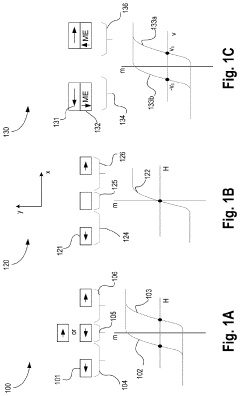
01 Spintronic memory devices with reduced access time
Spintronic memory technologies utilize spin-transfer torque or spin-orbit torque mechanisms to achieve faster switching speeds compared to traditional memory. These devices can reduce access time by employing magnetic tunnel junctions with optimized barrier layers and electrode configurations that enable rapid magnetization reversal. The implementation of perpendicular magnetic anisotropy and advanced material stacks further enhances the switching speed while maintaining data retention.- Spintronic memory devices with reduced access time: Spintronic memory technologies utilize spin-transfer torque or spin-orbit torque mechanisms to achieve faster switching speeds compared to traditional memory. These devices can reduce read and write access times through optimized magnetic tunnel junction structures and current-induced magnetization switching. The implementation of perpendicular magnetic anisotropy and reduced critical switching currents enables nanosecond-scale access times.
- MRAM architecture for improved memory access performance: Magnetoresistive random access memory architectures incorporate specialized cell designs and access circuitry to minimize latency. These architectures employ techniques such as hierarchical bit-line structures, sense amplifier optimization, and parallel access schemes. The integration of spin-based memory cells with CMOS technology enables competitive access times while maintaining non-volatility.
- Comparison of spintronic and conventional DRAM access mechanisms: Analysis of access time differences between spintronic memory and dynamic random access memory reveals trade-offs in speed, power consumption, and data retention. While traditional DRAM requires periodic refresh cycles that impact effective access time, spintronic alternatives offer non-volatile storage with potentially comparable read speeds. The evaluation includes considerations of cell capacitance, sense margin, and peripheral circuit delays.
- Cache memory integration with spintronic elements: Hybrid memory hierarchies combine spintronic memory elements with traditional cache structures to optimize overall system performance. These implementations leverage the fast access characteristics of SRAM for primary cache levels while utilizing spintronic memory for larger, non-volatile cache tiers. The integration strategies address latency matching, coherency protocols, and power management across different memory technologies.
- Access time optimization through material and device engineering: Enhancement of memory access speed through advanced materials selection and device structure optimization focuses on reducing resistance-area products and improving tunneling magnetoresistance ratios. Techniques include the use of novel magnetic materials, barrier layer engineering, and electrode optimization. These approaches aim to minimize read latency while maintaining adequate write speeds and thermal stability for reliable operation.
02 MRAM architecture for improved memory access performance
Magnetoresistive random access memory architectures incorporate specialized cell designs and access schemes to minimize latency. These architectures utilize optimized bit line and word line configurations, along with sense amplifier designs that enable faster read operations. The integration of reference cells and differential sensing techniques allows for rapid determination of memory states, significantly reducing overall access time compared to conventional memory technologies.Expand Specific Solutions03 Hybrid memory systems combining spintronic and traditional memory
Hybrid memory architectures leverage the advantages of both spintronic and traditional memory technologies to optimize overall system performance. These systems employ intelligent caching strategies and data management algorithms to place frequently accessed data in faster memory tiers. The combination allows for balancing speed, power consumption, and storage density, with spintronic elements providing non-volatility and traditional elements offering high-speed access for critical operations.Expand Specific Solutions04 Access time optimization through advanced read/write circuits
Specialized read and write circuitry designs enable faster memory access operations in both spintronic and traditional memory systems. These circuits incorporate pre-charging schemes, voltage regulation techniques, and timing optimization methods to reduce latency. Advanced sensing circuits with improved signal-to-noise ratios allow for faster detection of memory states, while write drivers with controlled current pulses enable rapid and reliable data storage operations.Expand Specific Solutions05 Memory controller and interface optimization for reduced latency
Memory controllers and interface protocols play a crucial role in determining effective access time. Advanced controller designs implement predictive algorithms, prefetching mechanisms, and parallel access schemes to minimize wait times. The optimization of command scheduling, bank management, and data path architectures enables more efficient utilization of memory bandwidth. These improvements apply to both spintronic and traditional memory systems, reducing the overall latency experienced by the processor.Expand Specific Solutions
Major Players in Spintronic and Memory Industry Landscape
The spintronics memory market represents an emerging technology sector in the early commercialization stage, transitioning from research-intensive development to practical applications. While traditional memory technologies dominate the multi-billion dollar global memory market, spintronics-based solutions like MRAM are gaining traction in specialized applications requiring non-volatility and radiation resistance. Technology maturity varies significantly across players: established semiconductor giants like Intel, Samsung Electronics, and Micron Technology leverage extensive R&D capabilities and manufacturing infrastructure, while specialized companies such as Everspin Technologies and Avalanche Technology focus exclusively on magnetic memory innovations. Research institutions including Beihang University, CNRS, and ITRI contribute fundamental breakthroughs, while foundries like TSMC and SMIC provide manufacturing support. The competitive landscape shows traditional memory leaders cautiously investing in spintronics while pure-play companies drive aggressive innovation, creating a dynamic environment where access time advantages could reshape memory hierarchies.
Intel Corp.
Technical Solution: Intel has developed advanced spintronic memory technologies including STT-MRAM and is researching next-generation spin-orbit torque (SOT) MRAM solutions[3]. Their spintronic memory implementations focus on achieving sub-10ns access times while maintaining non-volatility, targeting applications in cache memory and storage-class memory. Intel's approach combines traditional CMOS processing with magnetic tunnel junction (MTJ) integration, leveraging their advanced manufacturing capabilities to optimize both performance and cost-effectiveness. The company is also exploring hybrid memory architectures that combine spintronic elements with conventional memory technologies to achieve optimal access time versus capacity trade-offs[4].
Advantages: Advanced manufacturing capabilities, hybrid architecture optimization, sub-10ns access potential. Disadvantages: Still in development phase for commercial deployment, integration complexity with existing architectures.
Everspin Technologies, Inc.
Technical Solution: Everspin specializes in MRAM (Magnetoresistive Random Access Memory) technology, offering spintronic memory solutions with access times ranging from 35ns to 104ns for their Toggle MRAM and STT-MRAM products[1]. Their spintronic memory devices provide non-volatile storage with SRAM-like performance characteristics, enabling instant-on functionality and unlimited endurance. The company's STT-MRAM technology achieves faster switching speeds compared to traditional MRAM by using spin-transfer torque mechanisms, reducing power consumption while maintaining competitive access times against conventional SRAM and DRAM solutions[2].
Advantages: Non-volatile with SRAM-like speed, unlimited endurance, instant-on capability. Disadvantages: Higher cost per bit compared to traditional memory, limited density scalability.
Core Technologies in Spintronic Memory Access Speed
Access time calculator circuit, corresponding memory device and method
PatentPendingUS20250348214A1
Innovation
- A circuit and method using toggling of data read from the memory to generate a new clock, independent of external clocks, allowing for accurate access time measurement by counting reads at different addresses with a finite state machine.


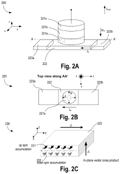
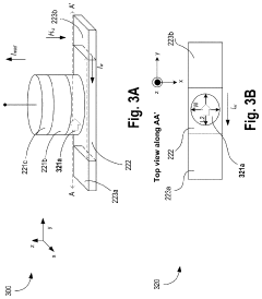
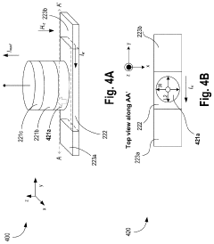
Spin orbit memory with multiferroic material
PatentActiveUS20190386202A1
Innovation
- A two-terminal memory bit-cell utilizing multiferroic materials, where the write electrode comprises heavy metals or antiferromagnetic materials with large spin-orbit torque to switch magnetization, decoupling read and write operations and enabling low-power, high-density memory storage.
Manufacturing Standards and Quality Control for Memory
Manufacturing standards for memory devices represent a critical differentiator between spintronic and traditional memory technologies, with each requiring distinct quality control frameworks due to their fundamentally different physical principles. Traditional memory manufacturing has benefited from decades of standardization through organizations like JEDEC and IEEE, establishing comprehensive specifications for DRAM, SRAM, and Flash memory production processes, materials, and performance metrics.
Spintronic memory manufacturing faces unique challenges in establishing standardized protocols due to the nascent nature of magnetic tunnel junction (MTJ) fabrication and spin-orbit torque devices. The precision required for magnetic layer deposition, typically measured in angstrom-level thickness control, demands specialized equipment and metrology tools that differ significantly from conventional semiconductor manufacturing. Current industry efforts focus on developing standardized test methodologies for magnetic properties, thermal stability, and endurance characteristics specific to spintronic devices.
Quality control parameters for traditional memory primarily emphasize electrical characteristics, defect density, and process uniformity across wafer lots. Established statistical process control methods monitor parameters such as threshold voltage distribution, leakage current, and retention time through well-defined test structures and accelerated aging protocols. These methodologies leverage mature understanding of silicon-based failure mechanisms and reliability physics.
Spintronic memory quality control introduces additional complexity through magnetic characterization requirements. Critical parameters include magnetic anisotropy uniformity, switching field distribution, and thermal stability factor measurements. The industry currently lacks standardized protocols for these magnetic properties, creating challenges for yield prediction and reliability assessment across different manufacturing facilities.
Contamination control represents another significant manufacturing consideration, where spintronic devices demonstrate heightened sensitivity to magnetic impurities compared to traditional memory. Specialized clean room protocols and material purity standards are emerging to address these requirements, though industry-wide adoption remains limited.
The integration of spintronic elements with CMOS processing requires hybrid manufacturing approaches that combine traditional semiconductor fabrication with specialized magnetic material deposition techniques. This integration necessitates new quality control frameworks that address both electrical and magnetic performance parameters simultaneously, representing a significant evolution from established memory manufacturing practices.
Energy Efficiency Considerations in Memory Design
Energy efficiency has emerged as a critical design parameter in modern memory systems, particularly when comparing spintronic-based memory technologies with traditional semiconductor memories. The fundamental energy consumption patterns differ significantly between these two approaches, with spintronics offering unique advantages in static power consumption while presenting distinct challenges in dynamic switching operations.
Traditional memory technologies, including SRAM, DRAM, and Flash, exhibit well-characterized energy profiles dominated by leakage currents and switching losses. SRAM maintains data through continuous current flow in cross-coupled inverters, resulting in substantial static power consumption that scales linearly with memory capacity. DRAM requires periodic refresh operations to maintain charge on storage capacitors, contributing to baseline energy overhead regardless of actual memory access patterns.
Spintronic memory devices fundamentally alter this energy landscape through their non-volatile nature and current-driven switching mechanisms. Spin-transfer torque (STT) and spin-orbit torque (SOT) based memories eliminate static power consumption entirely, as magnetic states persist without continuous energy input. This characteristic provides significant advantages in standby scenarios and battery-powered applications where idle power consumption directly impacts operational lifetime.
The dynamic energy requirements for spintronic memories present a more complex optimization challenge. Write operations in STT-MRAM require current densities sufficient to overcome magnetic anisotropy barriers, typically demanding 10-100 microamperes for switching durations of several nanoseconds. While instantaneous power levels may exceed those of traditional memories, the brief switching windows often result in lower total energy per write operation compared to Flash memory programming cycles.
Read operations in spintronic memories leverage magnetoresistive effects, requiring minimal current for state detection while maintaining non-destructive readout capabilities. This contrasts favorably with DRAM's destructive read operations that necessitate immediate write-back cycles, effectively doubling the energy cost of each read access.
Thermal considerations significantly influence energy efficiency comparisons, as spintronic devices typically exhibit improved temperature stability compared to charge-based storage mechanisms. Reduced temperature sensitivity translates to lower cooling requirements and more predictable energy consumption across varying operational environments, particularly relevant for data center and automotive applications where thermal management represents substantial energy overhead.
Unlock deeper insights with Patsnap Eureka Quick Research — get a full tech report to explore trends and direct your research. Try now!
Generate Your Research Report Instantly with AI Agent
Supercharge your innovation with Patsnap Eureka AI Agent Platform!