

Spintronics vs Photonics: Signal Processing Efficacy
APR 16, 20269 MIN READ
Generate Your Research Report Instantly with AI Agent
Patsnap Eureka helps you evaluate technical feasibility & market potential.
Spintronics vs Photonics Background and Processing Goals
The evolution of signal processing technologies has reached a critical juncture where traditional electronic approaches face fundamental limitations in speed, power consumption, and scalability. As data processing demands continue to exponentially increase across computing, telecommunications, and artificial intelligence applications, researchers have turned to alternative physical phenomena to overcome these constraints. Two emerging paradigms have gained significant attention: spintronics, which exploits electron spin properties, and photonics, which harnesses light-based information processing.
Spintronics represents a revolutionary approach that utilizes both the charge and spin degrees of freedom of electrons to process and store information. This field emerged from the discovery of giant magnetoresistance in the late 1980s and has since evolved to encompass spin-transfer torque devices, spin Hall effects, and magnetic tunnel junctions. The technology promises ultra-low power consumption, non-volatile memory capabilities, and compatibility with existing semiconductor infrastructure.
Photonics, conversely, leverages the unique properties of photons for signal processing, offering inherent advantages in bandwidth, processing speed, and electromagnetic interference immunity. Silicon photonics has matured significantly, enabling integration with complementary metal-oxide-semiconductor processes, while emerging materials like lithium niobate and indium phosphide provide enhanced electro-optic properties for advanced signal manipulation.
The primary objective of comparing these technologies centers on determining optimal signal processing efficacy across different application domains. Key performance metrics include processing speed, power efficiency, integration density, manufacturing scalability, and operational bandwidth. Understanding the fundamental trade-offs between these approaches is crucial for strategic technology investment decisions.
Current research aims to establish clear benchmarks for evaluating spintronics versus photonics in specific signal processing tasks such as analog computing, neuromorphic processing, and high-frequency communications. The goal extends beyond simple performance comparisons to identify synergistic opportunities where hybrid spintronic-photonic systems might deliver superior capabilities than either technology alone.
Market Demand for Advanced Signal Processing Solutions
The global signal processing market is experiencing unprecedented growth driven by the exponential increase in data generation and the demand for real-time processing capabilities across multiple industries. Traditional electronic signal processing systems are approaching fundamental physical limits, creating substantial market opportunities for revolutionary technologies like spintronics and photonics that can overcome these constraints.
Telecommunications infrastructure represents the largest market segment demanding advanced signal processing solutions. The deployment of 5G networks and the anticipated transition to 6G require processing capabilities that can handle massive data throughput with minimal latency. Current silicon-based processors struggle with the energy consumption and heat dissipation challenges at these scales, driving telecommunications companies to seek alternative technologies that can maintain performance while reducing operational costs.
Data centers and cloud computing facilities constitute another critical market segment experiencing acute signal processing demands. The proliferation of artificial intelligence applications, machine learning workloads, and big data analytics requires processing architectures that can handle parallel computations efficiently. These facilities face mounting pressure to reduce energy consumption while scaling processing capabilities, creating strong market pull for technologies that offer superior performance-per-watt ratios.
The automotive industry presents a rapidly expanding market for advanced signal processing, particularly with the development of autonomous vehicles and advanced driver assistance systems. These applications require real-time processing of sensor data from multiple sources including cameras, radar, and lidar systems. The stringent requirements for reliability, low latency, and energy efficiency in automotive environments create specific market niches where novel signal processing technologies can demonstrate clear advantages.
Defense and aerospace applications represent high-value market segments with specialized requirements for signal processing in challenging environments. These sectors demand solutions that can operate reliably under extreme conditions while providing superior performance for radar systems, electronic warfare applications, and satellite communications. The willingness to invest in cutting-edge technologies for strategic advantages makes these markets particularly attractive for emerging signal processing solutions.
Consumer electronics continue to drive volume demand for efficient signal processing capabilities. The integration of artificial intelligence features in smartphones, tablets, and IoT devices requires processing solutions that can deliver sophisticated functionality within strict power and thermal constraints. This market segment values technologies that can enable new user experiences while extending battery life and reducing device heating.
Current State and Challenges in Spin-Photonic Processing
The current landscape of spin-photonic processing represents a convergence of two distinct technological paradigms, each facing unique developmental challenges while offering complementary advantages for signal processing applications. Spintronics technology has achieved significant maturity in data storage applications, with spin-transfer torque magnetic random access memory (STT-MRAM) and giant magnetoresistance (GMR) sensors now commercially deployed. However, the transition from storage to active signal processing remains constrained by fundamental limitations in spin coherence times and energy dissipation rates.
Photonic signal processing has demonstrated exceptional capabilities in high-frequency applications, particularly in telecommunications and optical computing systems. Silicon photonics platforms have reached commercial viability for data center interconnects, achieving bandwidths exceeding 100 Gbps per channel. Nevertheless, photonic systems continue to struggle with miniaturization challenges and power consumption issues related to electro-optical conversion processes.
The integration of spintronic and photonic technologies faces several critical technical barriers. Spin-photon coupling mechanisms remain inefficient, with current magneto-optical effects achieving only modest modulation depths. The Faraday and Kerr effects, while well-understood, provide limited interaction strengths that constrain the development of compact spin-photonic devices. Additionally, the temporal mismatch between spin dynamics (nanosecond timescales) and optical processes (femtosecond timescales) creates synchronization challenges for hybrid processing architectures.
Material science constraints represent another significant challenge category. The development of materials exhibiting strong spin-orbit coupling while maintaining optical transparency requires precise engineering of heterostructures and interfaces. Current research focuses on topological insulators and two-dimensional materials, but scalable manufacturing processes for these exotic materials remain underdeveloped.
Geographically, spin-photonic research concentrates in advanced semiconductor manufacturing regions, with significant activities in Silicon Valley, European research consortiums, and Asian technology centers. The interdisciplinary nature of this field necessitates collaboration between traditionally separate research communities, creating coordination challenges that impact development timelines and standardization efforts.
System-level integration challenges persist in combining the distinct operational requirements of spintronic and photonic components. Thermal management, electromagnetic interference, and packaging considerations become increasingly complex when merging these technologies, particularly for applications requiring real-time signal processing capabilities with minimal latency constraints.
Current Signal Processing Solutions Comparison
01 Spintronic devices for signal processing and data manipulation
Spintronic devices utilize electron spin states for signal processing applications, enabling efficient data manipulation and storage. These devices leverage magnetic properties and spin-transfer torque effects to process signals with reduced power consumption compared to conventional electronics. The technology enables high-speed switching and non-volatile memory operations, making it suitable for advanced computing architectures and signal processing systems.- Spintronic devices for signal processing and modulation: Spintronic devices utilize electron spin properties to process and modulate signals with enhanced efficiency. These devices can manipulate spin states to achieve signal processing functions including amplification, switching, and modulation. The integration of magnetic materials and spin-dependent transport mechanisms enables low-power operation and high-speed signal processing capabilities. Spin-based modulators can control signal transmission through magnetic field manipulation or spin-orbit coupling effects.
- Photonic integrated circuits for signal processing: Photonic integrated circuits combine multiple optical components on a single substrate to perform complex signal processing operations. These circuits leverage light propagation and interference phenomena to achieve functions such as filtering, routing, and wavelength conversion. The integration of waveguides, resonators, and modulators enables compact and efficient signal processing systems. Advanced fabrication techniques allow for precise control of optical properties and enhanced processing performance.
- Hybrid spintronic-photonic integration for enhanced processing: Hybrid systems combine spintronic and photonic components to leverage advantages of both technologies for signal processing. These integrated platforms enable conversion between spin-based and optical signals, facilitating efficient data transfer and processing. The coupling of magnetic elements with optical waveguides allows for magneto-optical effects that can be exploited for signal manipulation. Such hybrid architectures offer potential for ultra-fast processing speeds and reduced energy consumption.
- Spin-wave based signal processing devices: Spin-wave devices utilize magnonic excitations for signal transmission and processing with minimal energy dissipation. These systems exploit the wave-like behavior of collective spin excitations in magnetic materials to perform computational operations. Spin-wave interference and propagation characteristics enable implementation of logic gates and signal processing functions. The non-volatile nature and scalability of spin-wave devices make them suitable for advanced computing applications.
- Optical switching and routing using spintronic control: Spintronic control mechanisms enable dynamic optical switching and routing for signal processing applications. Magnetic field modulation or spin-transfer torque effects can alter optical properties of materials to control light propagation paths. These switching systems offer fast response times and low insertion losses for optical signal management. Integration of spin-based control with photonic networks enhances flexibility and reconfigurability of signal routing architectures.
02 Photonic integrated circuits for signal processing
Photonic integrated circuits combine multiple optical components on a single chip to perform signal processing functions using light. These circuits offer advantages in bandwidth, speed, and power efficiency for processing high-frequency signals. The integration of waveguides, modulators, and detectors enables complex signal manipulation including filtering, switching, and routing operations in the optical domain.Expand Specific Solutions03 Hybrid spintronic-photonic systems for enhanced processing
Hybrid systems combine spintronic and photonic components to leverage advantages of both technologies for signal processing. These integrated platforms enable conversion between optical and spin-based signals, facilitating efficient data transfer and processing. The combination allows for novel functionalities including magneto-optical modulation and spin-photon coupling for advanced computing and communication applications.Expand Specific Solutions04 Optical modulators and switches for signal control
Advanced optical modulators and switches enable precise control of photonic signals for processing applications. These devices utilize various mechanisms including electro-optic, thermo-optic, and magneto-optic effects to manipulate light propagation and intensity. The technology supports high-speed signal routing, wavelength conversion, and amplitude modulation essential for optical communication and computing systems.Expand Specific Solutions05 Spin-wave based signal processing devices
Spin-wave devices utilize magnonic excitations for signal processing without charge transport, offering ultra-low power operation. These systems exploit spin wave propagation and interference in magnetic materials to perform logic operations and signal filtering. The technology enables nanoscale device integration and supports applications in analog computing, microwave signal processing, and neuromorphic architectures.Expand Specific Solutions
Key Players in Spintronics and Photonics Industries
The spintronics versus photonics signal processing landscape represents an emerging competitive arena where both technologies are transitioning from research phases toward commercial viability. The market remains fragmented with moderate growth potential, driven by increasing demands for high-speed, energy-efficient signal processing solutions. Technology maturity varies significantly between sectors, with photonics showing advanced development through companies like Sicoya, Lightmatter, and Photonic Systems specializing in optical communications and data center applications. Meanwhile, spintronics development is primarily concentrated within major semiconductor manufacturers including Intel, Samsung Electronics, TSMC, and IBM, who are integrating spin-based technologies into existing silicon platforms. The competitive dynamics favor established players with substantial R&D capabilities, though specialized photonics startups are gaining traction in niche applications.
Taiwan Semiconductor Manufacturing Co., Ltd.
Technical Solution: TSMC provides advanced manufacturing capabilities for both spintronic and photonic devices, enabling the production of next-generation signal processing components. Their spintronic manufacturing process supports magnetic tunnel junction fabrication with critical dimensions below 20nm, enabling high-density memory arrays with switching currents under 50 microamperes. TSMC's silicon photonics platform integrates optical components with electronic circuits using standard CMOS processes, achieving optical modulators with bandwidths exceeding 50 GHz and photodetectors with responsivities above 1 A/W. The company's heterogeneous integration capabilities allow for the co-packaging of spintronic memory, electronic logic, and photonic interconnects on single substrates.
Strengths: Advanced manufacturing processes, excellent yield rates, comprehensive integration capabilities. Weaknesses: Primarily a foundry service provider rather than technology developer, dependent on customer designs and specifications.
International Business Machines Corp.
Technical Solution: IBM has developed advanced spintronic technologies including magnetic tunnel junctions (MTJs) and spin-orbit torque devices for memory and logic applications. Their spintronic solutions demonstrate ultra-low power consumption with switching energies below 1 fJ per bit operation, enabling non-volatile memory with nanosecond access times. IBM's spintronic processors can achieve computational speeds comparable to traditional CMOS while maintaining persistent data storage capabilities. The company has also pioneered neuromorphic computing architectures using spintronic devices that mimic synaptic behavior for AI applications.
Strengths: Ultra-low power consumption, non-volatile operation, excellent scalability for memory applications. Weaknesses: Limited bandwidth compared to photonic solutions, slower switching speeds than optical systems.
Core Patents in Spin-Photonic Signal Processing
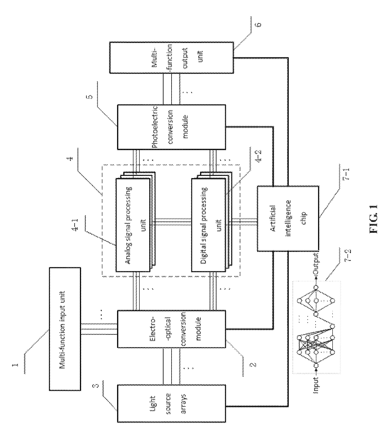
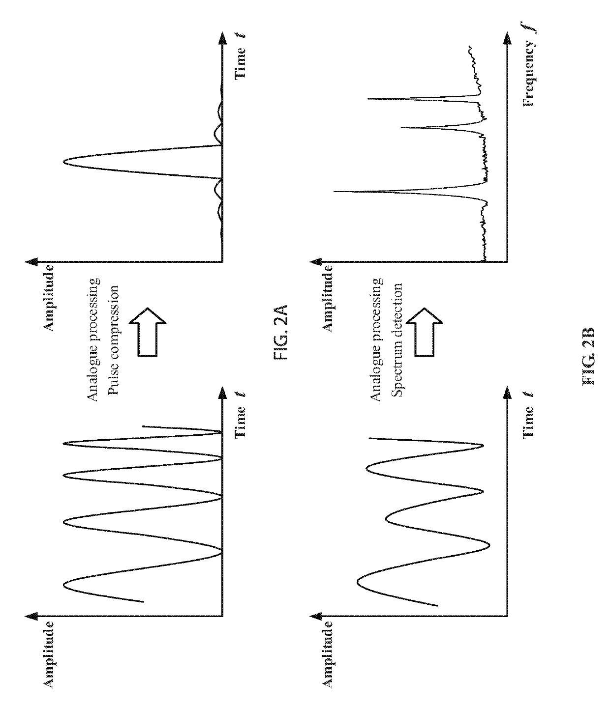
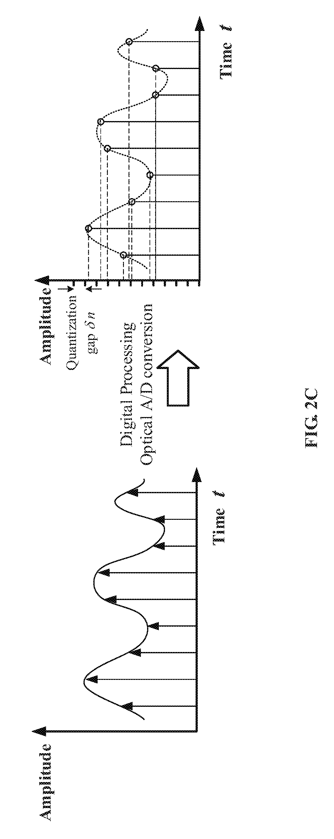
Method and system for intelligent decision-making photonic signal processing
PatentActiveUS20190318236A1
Innovation
- An intelligent decision-making photonic signal processing system combining photonic technology with deep learning, utilizing a multi-functional input unit, electro-optical conversion module, signal processing units, photoelectric conversion module, and an artificial intelligence chip to enable simultaneous digital and analog signal processing, leveraging heterogeneous photoelectron hybrid integration and packaging for real-time processing.

Energy Efficiency Standards for Signal Processing
Energy efficiency has emerged as a critical performance metric in evaluating signal processing technologies, with established standards providing benchmarks for comparing spintronics and photonics implementations. The IEEE 802.3 Energy Efficient Ethernet standard serves as a foundational reference, defining power consumption targets of less than 100mW per Gbps for high-speed data processing applications. These standards have been extended to encompass both electronic and optical signal processing domains.
Current energy efficiency standards for signal processing are primarily measured in terms of energy per bit (pJ/bit) and energy per operation (fJ/op). The International Technology Roadmap for Semiconductors (ITRS) has established target thresholds of 10 fJ/bit for switching operations and 1 pJ/bit for data transmission by 2030. These metrics provide quantitative frameworks for assessing the comparative performance of spintronic and photonic signal processing architectures.
Spintronic devices demonstrate compliance with emerging ultra-low power standards, particularly the IEEE P2415 standard for energy harvesting wireless sensor networks, which mandates sub-microwatt operational power levels. Magnetic tunnel junctions and spin-orbit torque devices typically operate within 0.1-1 fJ per switching event, positioning them favorably against conventional CMOS implementations that require 10-100 fJ per operation.
Photonic signal processing systems align with different efficiency standards, notably the ITU-T G.sup39 recommendations for optical transport networks, which specify maximum power consumption of 5W per 100Gbps throughput. Silicon photonic modulators achieve energy efficiencies of 50-200 fJ/bit, while advanced photonic integrated circuits demonstrate sub-10 fJ/bit performance in specific wavelength division multiplexing applications.
The emerging ISO/IEC 30134 standard for data center energy efficiency introduces new metrics specifically relevant to large-scale signal processing implementations. This standard emphasizes the importance of dynamic power scaling and idle-state power consumption, areas where both spintronic and photonic technologies show distinct advantages over traditional electronic approaches through their inherently low standby power characteristics.
Integration Challenges in Spin-Photonic Devices
The integration of spintronic and photonic components presents fundamental challenges that stem from the inherent differences between electronic and optical signal domains. The primary obstacle lies in achieving efficient spin-to-photon conversion while maintaining signal integrity across the interface. Current spin-photonic devices struggle with conversion efficiency rates typically below 10%, significantly limiting their practical implementation in high-performance signal processing applications.
Material compatibility represents another critical integration challenge. Spintronic devices typically rely on ferromagnetic materials and heavy metals with strong spin-orbit coupling, while photonic components require materials with specific optical properties such as low loss and high refractive index contrast. The thermal expansion coefficients, lattice parameters, and processing temperatures of these disparate materials often create mechanical stress and interface degradation during device fabrication.
Fabrication complexity emerges as a significant barrier due to the multi-step processing requirements. Spintronic components demand precise control of magnetic anisotropy and spin transport properties, while photonic structures require nanometer-scale dimensional accuracy for proper optical confinement. The sequential processing steps often involve incompatible temperature profiles and chemical environments, leading to performance degradation of previously fabricated components.
Signal synchronization poses substantial challenges in hybrid spin-photonic systems. Electronic spin signals operate on picosecond timescales, while photonic processing can achieve femtosecond response times. This temporal mismatch requires sophisticated buffering and timing control mechanisms, adding complexity to device architecture and potentially introducing latency that negates the speed advantages of photonic processing.
Packaging and interconnect challenges further complicate system-level integration. Spin-photonic devices require simultaneous electrical connections for spin control and optical coupling for photon manipulation. The packaging must maintain magnetic field isolation while providing optical access, often requiring specialized materials and assembly techniques that increase manufacturing costs and reduce yield rates.
Power management presents unique difficulties as spintronic components typically operate at low voltages with minimal power consumption, while photonic elements may require higher power laser sources and thermal management systems. Balancing these power requirements while maintaining overall system efficiency remains a significant engineering challenge that impacts the viability of integrated spin-photonic signal processing solutions.
Unlock deeper insights with Patsnap Eureka Quick Research — get a full tech report to explore trends and direct your research. Try now!
Generate Your Research Report Instantly with AI Agent
Supercharge your innovation with Patsnap Eureka AI Agent Platform!