Spintronics in Energy-Efficient Computation Infrastructure Development
APR 16, 20269 MIN READ
Generate Your Research Report Instantly with AI Agent
PatSnap Eureka helps you evaluate technical feasibility & market potential.
Spintronics Background and Energy-Efficient Computing Goals
Spintronics, also known as spin electronics, represents a revolutionary paradigm in electronic device technology that exploits the intrinsic spin of electrons alongside their fundamental charge property. This field emerged from the discovery of giant magnetoresistance (GMR) in the late 1980s, which demonstrated that electron spin could be manipulated to create dramatic changes in electrical resistance. The technology leverages quantum mechanical properties of electrons to achieve functionalities impossible with conventional charge-based electronics.
The historical development of spintronics began with theoretical foundations laid in the 1970s, followed by breakthrough experimental discoveries in magnetic multilayers. The field gained significant momentum with the development of spin-polarized transport phenomena and the subsequent realization of practical applications in magnetic storage devices. Today, spintronics encompasses a broad spectrum of phenomena including spin injection, spin transport, spin manipulation, and spin detection in various material systems.
Current technological evolution in spintronics focuses on developing devices that can process, store, and transmit information using electron spin states. Key developments include magnetic tunnel junctions, spin valves, and emerging concepts like spin-orbit torque devices and topological spintronic systems. These advances have enabled the creation of non-volatile memory devices, ultra-sensitive magnetic sensors, and novel logic circuits that combine memory and processing capabilities.
The primary goal of integrating spintronics into energy-efficient computation infrastructure centers on addressing the fundamental limitations of conventional CMOS technology. As Moore's Law approaches physical boundaries, traditional silicon-based computing faces escalating power consumption challenges, particularly in data centers and mobile computing platforms. Spintronics offers transformative solutions through non-volatile operation, reduced switching energy, and the potential for novel computing architectures.
Energy efficiency targets for spintronic computing systems include achieving sub-femtojoule switching energies, eliminating standby power consumption through non-volatile operation, and enabling instant-on computing capabilities. These objectives align with global sustainability initiatives and the growing demand for green computing solutions. The technology promises to deliver computational systems that maintain performance while dramatically reducing energy requirements, potentially revolutionizing everything from Internet-of-Things devices to high-performance computing clusters.
Market Demand for Energy-Efficient Computing Infrastructure
The global computing infrastructure market is experiencing unprecedented demand for energy-efficient solutions, driven by the exponential growth of data centers, cloud computing services, and artificial intelligence applications. Traditional silicon-based computing architectures are approaching their physical limits in terms of energy efficiency, creating a critical market gap that spintronics technology is positioned to address. Data centers currently consume substantial portions of global electricity, with cooling systems alone accounting for significant operational expenses, highlighting the urgent need for fundamentally more efficient computing paradigms.
Enterprise customers across various sectors are actively seeking computing solutions that can deliver higher performance while reducing power consumption and operational costs. The rise of edge computing, Internet of Things deployments, and real-time AI processing has intensified requirements for low-power, high-performance computing infrastructure. Organizations are increasingly prioritizing total cost of ownership calculations that factor in energy consumption, thermal management, and sustainability metrics when making infrastructure investment decisions.
The semiconductor industry faces mounting pressure to develop alternatives to conventional CMOS technology as Moore's Law scaling benefits diminish. Spintronics-based computing infrastructure offers compelling value propositions including non-volatile memory capabilities, reduced heat generation, and potential for ultra-low power operation. These characteristics align directly with market demands for always-on computing systems that maintain state without continuous power consumption.
Government initiatives and regulatory frameworks worldwide are accelerating adoption of energy-efficient technologies through incentives, standards, and environmental regulations. Carbon neutrality commitments from major technology companies are creating additional market pull for revolutionary computing architectures that can significantly reduce the environmental footprint of digital infrastructure.
The convergence of artificial intelligence workloads, quantum computing research, and neuromorphic computing applications is creating new market segments where spintronics technology can provide unique advantages. These emerging applications require computing architectures that can efficiently handle parallel processing, pattern recognition, and adaptive learning algorithms, areas where spintronic devices demonstrate particular promise for energy-efficient implementation.
Current State and Challenges of Spintronic Technologies
Spintronic technologies have emerged as a promising paradigm for next-generation computing systems, leveraging electron spin rather than charge for information processing and storage. The field has witnessed significant progress over the past two decades, with major breakthroughs in spin injection, manipulation, and detection mechanisms. Current spintronic devices demonstrate remarkable potential for ultra-low power consumption, non-volatile memory capabilities, and high-speed operation, positioning them as key enablers for energy-efficient computation infrastructure.
The global landscape of spintronic research reveals concentrated development in advanced semiconductor regions, particularly in the United States, Japan, South Korea, and several European nations. Leading research institutions and technology companies have established substantial intellectual property portfolios, with over 15,000 patents filed in spintronic-related technologies since 2010. Commercial applications have begun materializing in magnetic random-access memory (MRAM) and hard disk drive read heads, demonstrating the technology's transition from laboratory research to market-ready solutions.
Despite these achievements, spintronic technologies face several critical challenges that limit widespread adoption in computation infrastructure. Spin coherence remains a fundamental obstacle, as maintaining spin states over sufficient time periods and distances proves difficult at room temperature. Current spin diffusion lengths in most materials are inadequate for practical device scaling, typically ranging from nanometers to micrometers depending on the material system.
Material integration presents another significant hurdle, particularly in achieving efficient spin injection across dissimilar material interfaces. The conductivity mismatch problem continues to plague spintronic device performance, requiring sophisticated engineering solutions such as tunnel barriers or specialized contact materials. Manufacturing scalability poses additional constraints, as many promising spintronic materials require precise atomic-level control and exotic fabrication conditions incompatible with standard semiconductor processing.
Thermal stability and reliability concerns further complicate practical implementation. Many spintronic phenomena exhibit strong temperature dependencies, potentially limiting operational ranges in real-world computing environments. Device-to-device variability and long-term stability under electrical stress remain inadequately characterized for mission-critical applications.
Power consumption advantages, while theoretically substantial, have not yet been fully realized in practical systems due to peripheral circuit requirements and switching energy considerations. The integration of spintronic components with conventional CMOS technology presents architectural challenges that require innovative hybrid design approaches to maximize energy efficiency benefits while maintaining computational performance standards.
Current Spintronic Solutions for Energy-Efficient Computing
01 Spin-transfer torque magnetoresistive devices for low-power memory
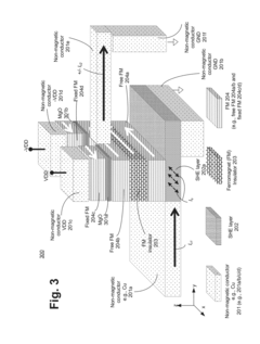
Spin-transfer torque (STT) technology enables magnetoresistive random-access memory (MRAM) devices that consume significantly less power compared to conventional memory technologies. These devices utilize spin-polarized currents to switch magnetic states with minimal energy expenditure, making them ideal for energy-efficient computing applications. The technology allows for non-volatile data storage with reduced write currents and faster switching speeds, contributing to overall system energy efficiency.- Spin-transfer torque magnetoresistive devices for low-power memory: Spin-transfer torque (STT) technology enables magnetoresistive random-access memory (MRAM) devices that consume significantly less power compared to conventional memory technologies. These devices utilize spin-polarized currents to switch magnetic states with minimal energy expenditure, making them ideal for energy-efficient computing applications. The technology allows for non-volatile data storage with reduced write currents and faster switching speeds.
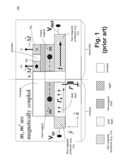
- Spintronic logic devices with reduced energy consumption: Spintronic logic circuits leverage electron spin rather than charge to perform computational operations, resulting in substantial energy savings. These devices can operate at lower voltages while maintaining high performance, reducing overall power dissipation in integrated circuits. The implementation of spin-based logic gates enables energy-efficient processing architectures suitable for mobile and embedded systems.
- Magnetic tunnel junction structures for energy-efficient data storage: Magnetic tunnel junctions (MTJs) provide energy-efficient data storage solutions by exploiting tunneling magnetoresistance effects. These structures enable low-power read and write operations while maintaining high data retention and endurance. Advanced MTJ designs incorporate optimized barrier layers and electrode materials to minimize energy consumption during switching operations.
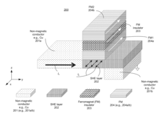
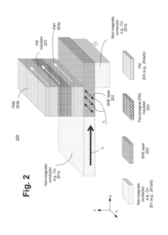
- Spin Hall effect devices for efficient spin current generation: Spin Hall effect-based devices convert charge currents into spin currents with high efficiency, enabling low-power spintronic applications. These structures utilize materials with strong spin-orbit coupling to generate and manipulate spin currents without the need for ferromagnetic components. The technology offers pathways for creating energy-efficient spin torque oscillators and detectors.
- Antiferromagnetic spintronic devices for ultra-low power operation: Antiferromagnetic materials enable spintronic devices with ultra-low power consumption due to their lack of stray magnetic fields and ultrafast dynamics. These devices can operate at terahertz frequencies while consuming minimal energy, making them suitable for next-generation computing architectures. The use of antiferromagnetic elements reduces energy losses associated with magnetic field generation and provides enhanced stability.
02 Magnetic tunnel junction structures with optimized energy barriers
Advanced magnetic tunnel junction (MTJ) designs incorporate optimized barrier layers and electrode configurations to minimize energy consumption during read and write operations. These structures achieve improved tunneling magnetoresistance ratios while reducing the critical switching current density. The optimization of material composition and layer thickness enables lower operating voltages and enhanced thermal stability, resulting in more energy-efficient spintronic devices suitable for high-density memory arrays.Expand Specific Solutions03 Spin-orbit torque devices for reduced power consumption
Spin-orbit torque (SOT) mechanisms provide an alternative switching method that can achieve lower energy consumption compared to traditional spin-transfer torque approaches. These devices exploit the spin-orbit coupling effect in heavy metal layers to generate efficient spin currents for magnetization switching. The separation of read and write paths in SOT devices enables independent optimization of each operation, leading to improved endurance and reduced energy requirements for memory and logic applications.Expand Specific Solutions04 Spintronic logic circuits with ultra-low power operation
Spintronic-based logic devices leverage magnetic states for information processing, offering non-volatile operation and near-zero standby power consumption. These circuits combine magnetic tunnel junctions with complementary metal-oxide-semiconductor (CMOS) technology to create hybrid architectures that maintain logic states without continuous power supply. The integration enables instant-on computing capabilities and dramatic reductions in static power dissipation, making them particularly suitable for energy-constrained applications and Internet of Things devices.Expand Specific Solutions05 Antiferromagnetic spintronic devices for enhanced efficiency
Antiferromagnetic materials in spintronic applications offer advantages including ultrafast dynamics, insensitivity to external magnetic fields, and potential for higher integration density. These devices exploit the properties of antiferromagnetic ordering to achieve energy-efficient switching and data storage with minimal stray field effects. The use of antiferromagnetic components enables operation at higher frequencies with lower power consumption compared to ferromagnetic counterparts, opening new possibilities for next-generation energy-efficient computing architectures.Expand Specific Solutions
Key Players in Spintronics and Computing Industry
The spintronics field for energy-efficient computation infrastructure is in an emerging growth phase, transitioning from laboratory research to early commercial applications. The market represents a nascent but rapidly expanding segment within the broader semiconductor industry, driven by increasing demands for low-power computing solutions in data centers and mobile devices. Technology maturity varies significantly across key players, with established semiconductor giants like Intel Corp. and IBM demonstrating advanced research capabilities and prototype development, while companies such as SK hynix NAND Product Solutions Corp. and Cisco Technology Inc. focus on integrating spintronic principles into existing product lines. Academic institutions including University of California, McGill University, and various Chinese universities contribute fundamental research breakthroughs. The competitive landscape shows a hybrid ecosystem where traditional tech companies collaborate with research institutions to accelerate commercialization, though widespread market adoption remains 3-5 years away pending manufacturing scalability improvements.
Intel Corp.
Technical Solution: Intel has developed comprehensive spintronics solutions focusing on spin-transfer torque magnetic random access memory (STT-MRAM) and spin-orbit torque devices for energy-efficient computing infrastructure. Their approach integrates magnetoresistive tunnel junctions with CMOS technology to create non-volatile memory solutions that consume significantly less power than traditional SRAM and DRAM. Intel's spintronics research emphasizes reducing switching energy through optimized magnetic materials and device architectures, achieving sub-nanosecond switching speeds while maintaining data retention for over 10 years. Their technology roadmap includes integration of spintronic devices in cache memory systems and neuromorphic computing applications, targeting 10x energy efficiency improvements in data center operations.
Strengths: Strong CMOS integration capabilities, extensive manufacturing infrastructure, proven track record in memory technologies. Weaknesses: Limited commercialization of spintronics products, high development costs, competition from established memory technologies.
The Regents of the University of California
Technical Solution: UC system has conducted groundbreaking spintronics research focusing on spin-orbit torque devices and topological spintronic materials for energy-efficient quantum and classical computing applications. Their research encompasses development of chiral magnetic structures and antiferromagnetic spintronics that promise ultra-fast switching speeds with minimal energy dissipation. The university's spintronics program investigates novel phenomena such as spin Hall effect and Rashba effect in heterostructures for creating energy-efficient spin-based transistors and memory devices. Their technology platform includes exploration of magnonic computing concepts where spin waves carry information with significantly lower energy consumption than electronic charge transport. UC researchers have demonstrated prototype spintronic devices operating at room temperature with switching energies approaching thermodynamic limits.
Strengths: World-class research facilities, leading scientific expertise, strong publication record, extensive collaboration networks with industry and government. Weaknesses: Limited manufacturing capabilities, focus on fundamental research rather than commercial applications, technology transfer barriers, long development timelines.
Core Spintronic Innovations for Low-Power Computing
Magnetoelectric spin-orbit device with in-plane and perpendicular magnetic layers and method of manufacturing same
PatentActiveUS20230284538A1
Innovation
- The proposed solution involves using a perpendicular magnetic anisotropy (PMA) magnet in conjunction with the anomalous Hall effect to improve readout voltage and simplify manufacturing by employing a magnetoelectric spin-orbit (MESO) device with a ferroelectric material instead of ferromagnetic materials, allowing for easier integration and faster operation.
Spin logic with magnetic insulators switched by spin orbit coupling
PatentActiveUS20180240964A1
Innovation
- The use of ferromagnets with strong exchange coupling and a composite nanomagnet structure, comprising two FM metal layers separated by an insulating FM layer, along with a spin orbit coupling layer and a FM insulator, to enhance switching speed and reliability.
Environmental Impact Assessment of Spintronic Technologies
The environmental implications of spintronic technologies represent a critical consideration in their development and deployment for energy-efficient computation infrastructure. Unlike traditional semiconductor manufacturing, spintronic device fabrication requires specialized materials including rare earth elements and heavy metals such as platinum, cobalt, and gadolinium. The extraction and processing of these materials pose significant environmental challenges, particularly in mining operations that can lead to soil contamination and water pollution in extraction regions.
Manufacturing processes for spintronic devices involve sophisticated thin-film deposition techniques, including molecular beam epitaxy and sputtering, which consume substantial energy and utilize potentially hazardous chemicals. However, the environmental footprint during production is partially offset by the inherently lower material requirements compared to conventional CMOS technologies, as spintronic devices can achieve similar functionality with reduced physical dimensions and material volumes.
The operational environmental benefits of spintronic technologies are substantial, primarily stemming from their dramatically reduced power consumption characteristics. Magnetic tunnel junctions and spin-based memory devices can operate at power levels orders of magnitude lower than traditional electronic components, potentially reducing data center energy consumption by 30-50%. This reduction translates directly to decreased carbon emissions from power generation, particularly significant given that global data centers currently account for approximately 1% of worldwide electricity consumption.
End-of-life considerations for spintronic devices present both challenges and opportunities. The presence of rare earth elements necessitates specialized recycling processes to recover valuable materials and prevent environmental contamination. However, the reduced complexity and material diversity in spintronic devices compared to conventional electronics may facilitate more efficient recycling protocols.
Life cycle assessments indicate that despite higher initial environmental costs during material extraction and manufacturing, the extended operational phase benefits of spintronic technologies result in a net positive environmental impact over typical device lifespans of 10-15 years, making them environmentally favorable for large-scale computational infrastructure deployment.
Manufacturing Scalability of Spintronic Devices
The manufacturing scalability of spintronic devices represents one of the most critical bottlenecks in transitioning from laboratory demonstrations to commercial energy-efficient computation infrastructure. Current fabrication processes for spintronic components, including magnetic tunnel junctions (MTJs) and spin-orbit torque devices, rely heavily on sophisticated thin-film deposition techniques such as magnetron sputtering and molecular beam epitaxy. These methods, while enabling precise control over material properties and interface quality, present significant challenges when scaling to high-volume production due to their inherently slow deposition rates and complex multi-step processing requirements.
The uniformity control across large-area substrates poses another fundamental challenge in spintronic device manufacturing. Maintaining consistent magnetic properties, tunnel barrier thickness, and crystalline orientation across 300mm wafers requires unprecedented precision in process control. Variations in these parameters directly impact device performance metrics such as tunnel magnetoresistance ratio, switching current density, and thermal stability, making yield optimization particularly challenging compared to conventional semiconductor devices.
Integration compatibility with existing CMOS fabrication infrastructure represents a crucial consideration for manufacturing scalability. Spintronic devices must withstand standard semiconductor processing temperatures, typically up to 400°C, while preserving their magnetic characteristics. The thermal budget constraints limit material choices and annealing procedures, often requiring novel low-temperature processing techniques that may not be readily compatible with established manufacturing workflows.
Material supply chain considerations further complicate scalability prospects. Many high-performance spintronic devices rely on rare earth elements or exotic magnetic alloys with limited global availability. The development of alternative material systems using abundant elements, while maintaining comparable performance characteristics, becomes essential for large-scale deployment in computation infrastructure.
Process standardization and quality control methodologies specific to spintronic manufacturing remain underdeveloped compared to traditional semiconductor processes. The magnetic nature of these devices requires specialized metrology tools and testing protocols that can accurately characterize spin-dependent transport properties at the wafer level, adding complexity and cost to the manufacturing process.
Unlock deeper insights with PatSnap Eureka Quick Research — get a full tech report to explore trends and direct your research. Try now!
Generate Your Research Report Instantly with AI Agent
Supercharge your innovation with PatSnap Eureka AI Agent Platform!