

How to Synchronize Spintronics with Next-Generation Rapid Prototyping
APR 16, 20269 MIN READ
Generate Your Research Report Instantly with AI Agent
PatSnap Eureka helps you evaluate technical feasibility & market potential.
Spintronics and Rapid Prototyping Integration Background
Spintronics, a revolutionary field that exploits the intrinsic spin of electrons alongside their charge, has emerged as a cornerstone technology for next-generation electronic devices. This quantum mechanical property enables the development of devices with enhanced functionality, reduced power consumption, and non-volatile memory capabilities. The field has evolved from fundamental research in the 1980s to practical applications in modern hard disk drives and magnetic random-access memory systems.
The convergence of spintronics with rapid prototyping technologies represents a paradigm shift in how magnetic and spin-based devices are conceptualized, designed, and manufactured. Traditional spintronics device fabrication relies heavily on cleanroom environments, lithographic processes, and specialized deposition techniques that require significant time and capital investment. These conventional approaches often create barriers between theoretical design and practical implementation, limiting innovation cycles.
Rapid prototyping technologies, including additive manufacturing, direct-write techniques, and advanced material deposition systems, have demonstrated remarkable capabilities in producing complex geometries and multi-material structures with unprecedented speed and flexibility. The integration of these technologies with spintronics opens new possibilities for creating sophisticated magnetic devices, sensors, and memory systems that were previously difficult or impossible to fabricate using traditional methods.
The synchronization challenge arises from the fundamental differences between spintronics requirements and rapid prototyping capabilities. Spintronics devices demand precise control over magnetic properties, crystalline structures, and interface quality at nanoscale dimensions. Meanwhile, rapid prototyping excels in creating macroscale structures with complex geometries but traditionally lacks the resolution and material control necessary for spintronic applications.
Recent technological advances have begun bridging this gap through developments in high-resolution 3D printing of magnetic materials, direct laser writing of spin-active structures, and hybrid manufacturing approaches that combine rapid prototyping with precision deposition techniques. These innovations are creating opportunities for accelerated development cycles, customized device architectures, and novel applications that leverage both the unique properties of spintronic materials and the design freedom offered by rapid prototyping.
The integration represents a transformative approach that could democratize spintronics research and development, enabling rapid iteration of device designs and facilitating the exploration of unconventional architectures that traditional manufacturing methods cannot easily accommodate.
Market Demand for Spintronic Rapid Prototyping Solutions
The convergence of spintronics and rapid prototyping technologies represents a rapidly emerging market segment driven by the semiconductor industry's urgent need for faster, more efficient device development cycles. Traditional electronic prototyping methods face significant limitations when dealing with spintronic devices, which manipulate electron spin rather than charge, creating substantial demand for specialized rapid prototyping solutions that can handle magnetic properties and spin-dependent phenomena.
The quantum computing sector stands as a primary driver of market demand, where spintronic components serve as fundamental building blocks for quantum bits and quantum gates. Research institutions and technology companies developing quantum processors require rapid prototyping capabilities to iterate quickly through spintronic qubit designs, test magnetic coupling mechanisms, and optimize spin coherence times. This demand intensifies as quantum computing transitions from laboratory research to commercial applications.
Memory and storage technology markets present another significant demand source. Next-generation magnetic random-access memory (MRAM), spin-transfer torque memory (STT-RAM), and other spintronic storage devices require sophisticated prototyping tools capable of fabricating and testing magnetic tunnel junctions, spin valves, and domain wall devices. The growing need for non-volatile, high-speed memory solutions in data centers and edge computing applications amplifies this market segment.
The automotive and industrial IoT sectors increasingly demand spintronic sensors and actuators for advanced driver assistance systems, autonomous vehicles, and smart manufacturing equipment. These applications require rapid prototyping solutions that can integrate magnetic sensing elements with traditional semiconductor processing, enabling faster development of magnetoresistive sensors, spin-based gyroscopes, and magnetic field detectors.
Emerging applications in neuromorphic computing and artificial intelligence hardware create additional market pressure. Spintronic devices offer unique advantages for implementing synaptic functions and neural network architectures, but require specialized prototyping environments that can simulate and fabricate spin-based artificial neurons and synapses.
The market demand is further intensified by the need for multi-physics simulation capabilities that can simultaneously model electrical, magnetic, and thermal properties during the prototyping phase, enabling comprehensive validation of spintronic device performance before full-scale manufacturing.
Current Challenges in Spintronics Manufacturing Speed
The manufacturing speed of spintronic devices represents one of the most significant bottlenecks preventing widespread commercial adoption of this promising technology. Current fabrication processes for spintronic components rely heavily on traditional semiconductor manufacturing techniques, which were not originally designed to handle the unique requirements of spin-based electronics. These conventional methods often require multiple sequential processing steps, each demanding precise control over magnetic properties, crystalline structures, and interface quality.
Lithography limitations pose substantial challenges when creating nanoscale spintronic structures. The need for extremely fine feature sizes, often below 10 nanometers, pushes current photolithography and electron-beam lithography systems to their operational limits. This results in significantly reduced throughput compared to conventional semiconductor manufacturing, as each device requires extended exposure times and multiple alignment steps to achieve the necessary precision.
Material deposition processes for spintronic devices face unique speed constraints due to the requirement for maintaining specific magnetic orientations and minimizing defects at material interfaces. Techniques such as molecular beam epitaxy and sputtering, while capable of producing high-quality magnetic thin films, operate at substantially slower rates than standard semiconductor deposition methods. The need for ultra-high vacuum conditions and precise temperature control further extends processing times.
Thermal processing steps present additional manufacturing speed challenges, as spintronic materials often require carefully controlled annealing procedures to achieve desired magnetic properties. These thermal treatments typically involve slow heating and cooling cycles to prevent the formation of unwanted phases or the degradation of magnetic interfaces. Such extended thermal processing can add hours to the manufacturing cycle for each device batch.
Quality control and characterization procedures significantly impact manufacturing throughput in spintronics production. Unlike conventional electronics, spintronic devices require specialized testing of magnetic properties, spin polarization, and magnetoresistance characteristics. These measurements often involve complex magnetic field applications and temperature variations, making inline testing substantially more time-consuming than standard electrical characterization methods.
The integration of multiple magnetic materials with different processing requirements creates additional manufacturing complexity. Each material layer may require distinct deposition conditions, annealing temperatures, and etching chemistries, preventing the use of batch processing techniques that accelerate conventional semiconductor manufacturing. This sequential processing approach fundamentally limits the potential for high-volume production.
Current manufacturing equipment designed for spintronic device fabrication lacks the automation and parallel processing capabilities found in mature semiconductor production lines. Most spintronic manufacturing relies on research-grade equipment that prioritizes precision over speed, resulting in significantly lower wafer throughput compared to established semiconductor fabrication facilities.
Existing Rapid Prototyping Methods for Spintronic Devices
01 Spin-torque oscillators for synchronization
Spin-torque oscillators utilize spin-polarized currents to generate oscillations in magnetic layers, which can be synchronized through mutual coupling or external signals. These devices exploit the spin-transfer torque effect where electrons transfer angular momentum to magnetic moments, enabling phase-locking and frequency synchronization. The synchronization can be achieved through electrical or magnetic coupling between multiple oscillators, allowing for coherent operation and enhanced output power in spintronic applications.- Spin-torque oscillators for synchronization: Spin-torque oscillators utilize spin-polarized currents to generate oscillations in magnetic layers, which can be synchronized for various applications. These devices exploit the spin-transfer torque effect where electrons transfer angular momentum to magnetic moments, causing precession. Multiple oscillators can be coupled to achieve phase-locking and synchronized operation, enabling applications in signal processing and communication systems.
- Magnetic tunnel junctions for synchronized spintronic devices: Magnetic tunnel junctions serve as fundamental building blocks for spintronic synchronization by utilizing tunneling magnetoresistance effects. These structures consist of two ferromagnetic layers separated by a thin insulating barrier, allowing spin-dependent electron tunneling. The resistance state can be controlled and synchronized through external magnetic fields or spin currents, enabling coherent operation of multiple devices for memory and logic applications.
- Phase-locked loop circuits with spintronic elements: Integration of spintronic components into phase-locked loop architectures enables synchronization of oscillating signals with improved performance characteristics. These circuits utilize magnetic properties and spin dynamics to achieve frequency and phase alignment between reference and output signals. The incorporation of spintronic elements provides advantages such as reduced power consumption, enhanced stability, and compatibility with existing semiconductor technologies.
- Spin wave-based synchronization mechanisms: Spin waves or magnons propagating through magnetic materials provide a mechanism for achieving synchronization in spintronic systems. These collective excitations of magnetic moments can carry information and enable coupling between distant spintronic devices. The wave-based approach allows for non-local synchronization effects and can be controlled through material properties, geometry, and external fields, offering potential for novel computing architectures.
- Voltage-controlled magnetic anisotropy for synchronization control: Voltage-controlled magnetic anisotropy enables electrical manipulation of magnetic properties for achieving and controlling synchronization in spintronic devices. By applying voltage across magnetic structures, the magnetic anisotropy can be modulated, affecting the precession dynamics and coupling between oscillators. This approach offers energy-efficient control of synchronization states and enables dynamic reconfiguration of coupled spintronic systems for adaptive applications.
02 Magnetic tunnel junctions for synchronized operations
Magnetic tunnel junctions serve as fundamental building blocks for spintronic synchronization by utilizing the tunneling magnetoresistance effect. These structures consist of two ferromagnetic layers separated by a thin insulating barrier, where the resistance depends on the relative magnetization alignment. Synchronization is achieved through spin-wave propagation and exchange coupling between adjacent junctions, enabling coordinated switching and oscillation patterns for neuromorphic computing and memory applications.Expand Specific Solutions03 Phase-locked loop circuits with spintronic elements
Phase-locked loop architectures incorporating spintronic components enable precise frequency and phase synchronization in magnetic devices. These circuits utilize feedback mechanisms to lock the phase of spin-based oscillators to reference signals, maintaining stable synchronization even under varying operating conditions. The integration of magnetic elements with conventional electronic circuits provides low-power synchronization solutions with enhanced noise immunity and temperature stability.Expand Specific Solutions04 Spin wave-based synchronization mechanisms
Spin waves propagating through magnetic media provide a mechanism for achieving synchronization across spintronic devices without direct electrical connections. These collective excitations of magnetic moments can couple multiple oscillators or memory elements through dipolar or exchange interactions, enabling parallel synchronization of large arrays. The wave-based approach offers advantages in terms of scalability and energy efficiency for distributed spintronic systems.Expand Specific Solutions05 Voltage-controlled magnetic anisotropy for synchronization control
Voltage-controlled magnetic anisotropy enables dynamic tuning of magnetic properties through electric fields, providing a mechanism for controlling synchronization in spintronic systems. This approach modulates the magnetic anisotropy energy at interfaces between magnetic and dielectric layers, allowing for low-power adjustment of oscillation frequencies and phase relationships. The voltage control mechanism facilitates adaptive synchronization schemes and reduces power consumption compared to current-driven methods.Expand Specific Solutions
Key Players in Spintronics and Prototyping Industries
The synchronization of spintronics with next-generation rapid prototyping represents an emerging technological convergence in its early development stage. The market remains nascent with limited commercial applications, primarily driven by research institutions and technology companies exploring quantum computing and advanced manufacturing integration. Technology maturity varies significantly across key players: established semiconductor companies like Texas Instruments and ASML Netherlands possess foundational expertise in precision manufacturing, while research institutions including Tsinghua University, Huazhong University of Science & Technology, and Industrial Technology Research Institute are advancing fundamental spintronic principles. Industrial automation specialists such as Siemens AG and Shanghai Step Electric are developing complementary rapid prototyping capabilities. The competitive landscape shows fragmented development with no dominant market leader, as companies like Honor Device and various Chinese research institutes pursue parallel development paths in quantum-enabled manufacturing technologies.
Tsinghua University
Technical Solution: Tsinghua University conducts cutting-edge research in spintronic materials and devices, developing novel approaches for integrating spin-based technologies with rapid prototyping methodologies. Their research focuses on two-dimensional magnetic materials, topological insulators, and spin-orbit torque devices. The university has established advanced fabrication facilities including molecular beam epitaxy systems and electron beam lithography for creating spintronic prototypes. Their interdisciplinary approach combines materials science, quantum physics, and engineering to develop scalable manufacturing processes for next-generation spintronic applications including neuromorphic computing and quantum information processing.
Strengths: Leading fundamental research capabilities and state-of-the-art fabrication facilities for novel spintronic materials. Weaknesses: Limited commercial manufacturing experience and technology transfer capabilities compared to industry players.
Texas Instruments Incorporated
Technical Solution: Texas Instruments develops specialized analog and mixed-signal processing solutions that interface with spintronic devices for rapid prototyping applications. Their high-speed ADCs and precision amplifiers enable real-time measurement of magnetoresistance changes and spin-dependent transport properties during device characterization. The company's embedded processing platforms support machine learning algorithms for automated optimization of spintronic device parameters, while their power management ICs provide the ultra-low noise power supplies essential for sensitive magnetic measurements in prototyping environments.
Strengths: Extensive analog signal processing expertise and robust semiconductor manufacturing capabilities. Weaknesses: Limited direct involvement in spintronic material science and quantum device physics research.
Core Technologies for Spintronics-Prototyping Synchronization
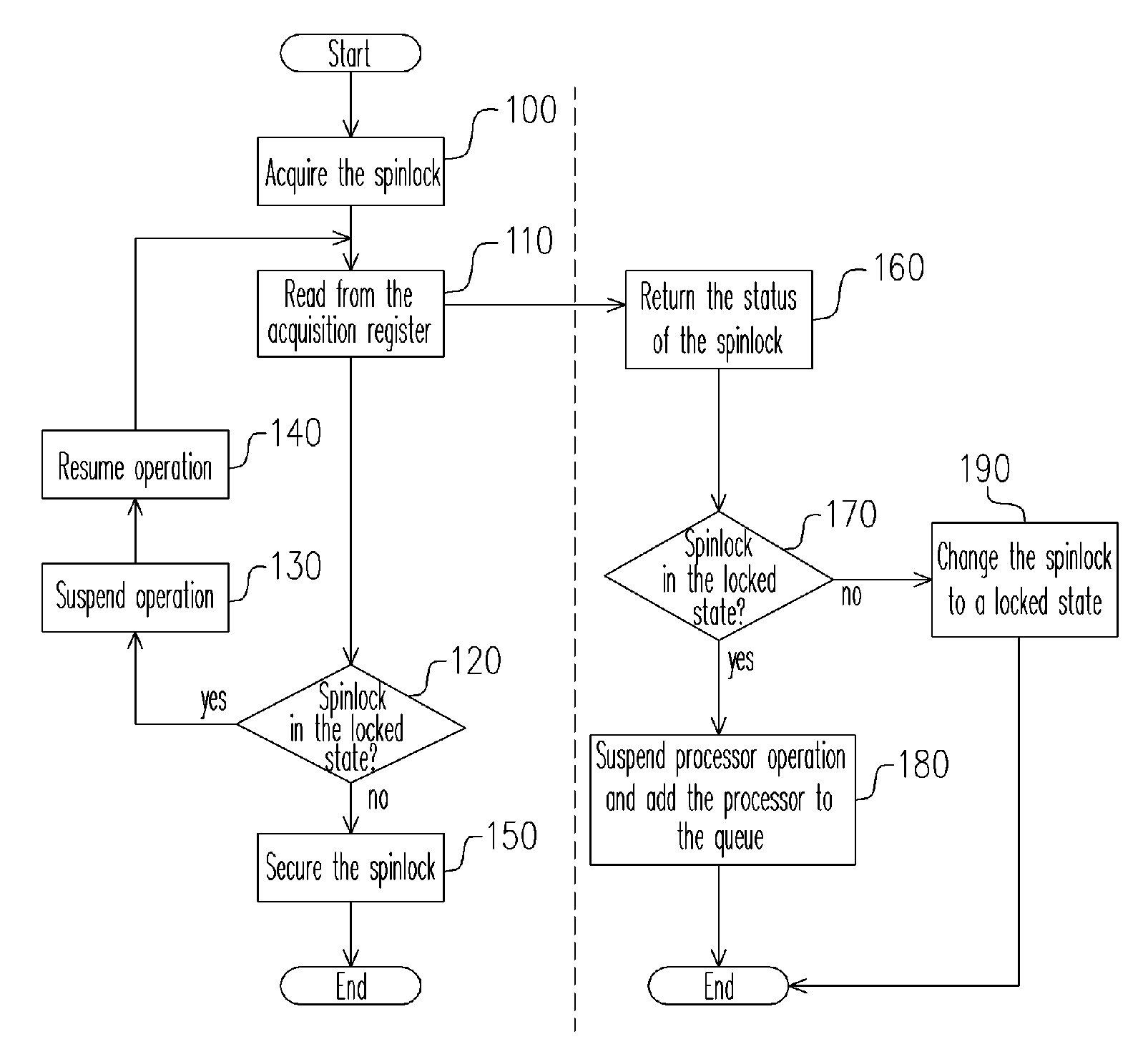
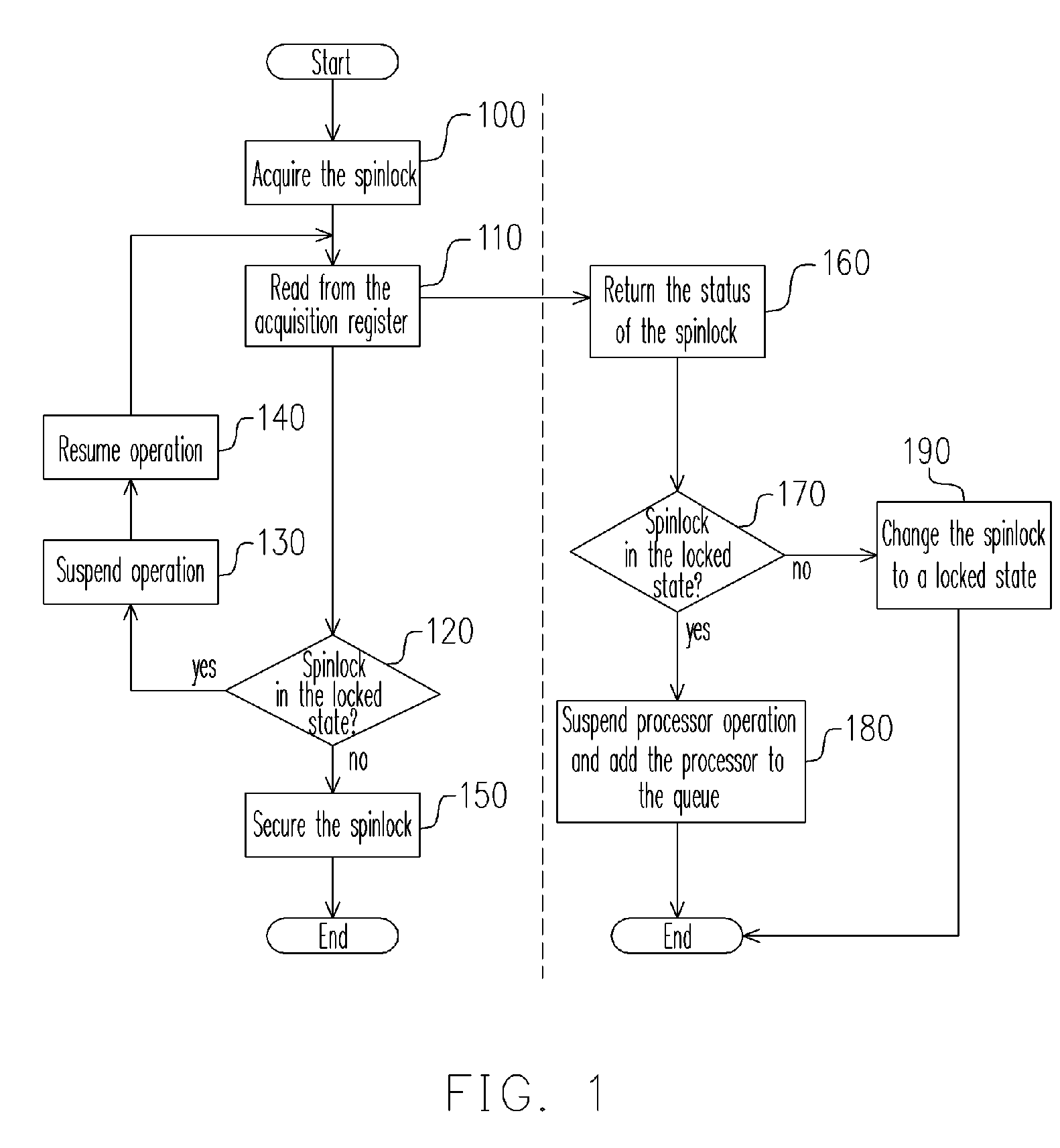
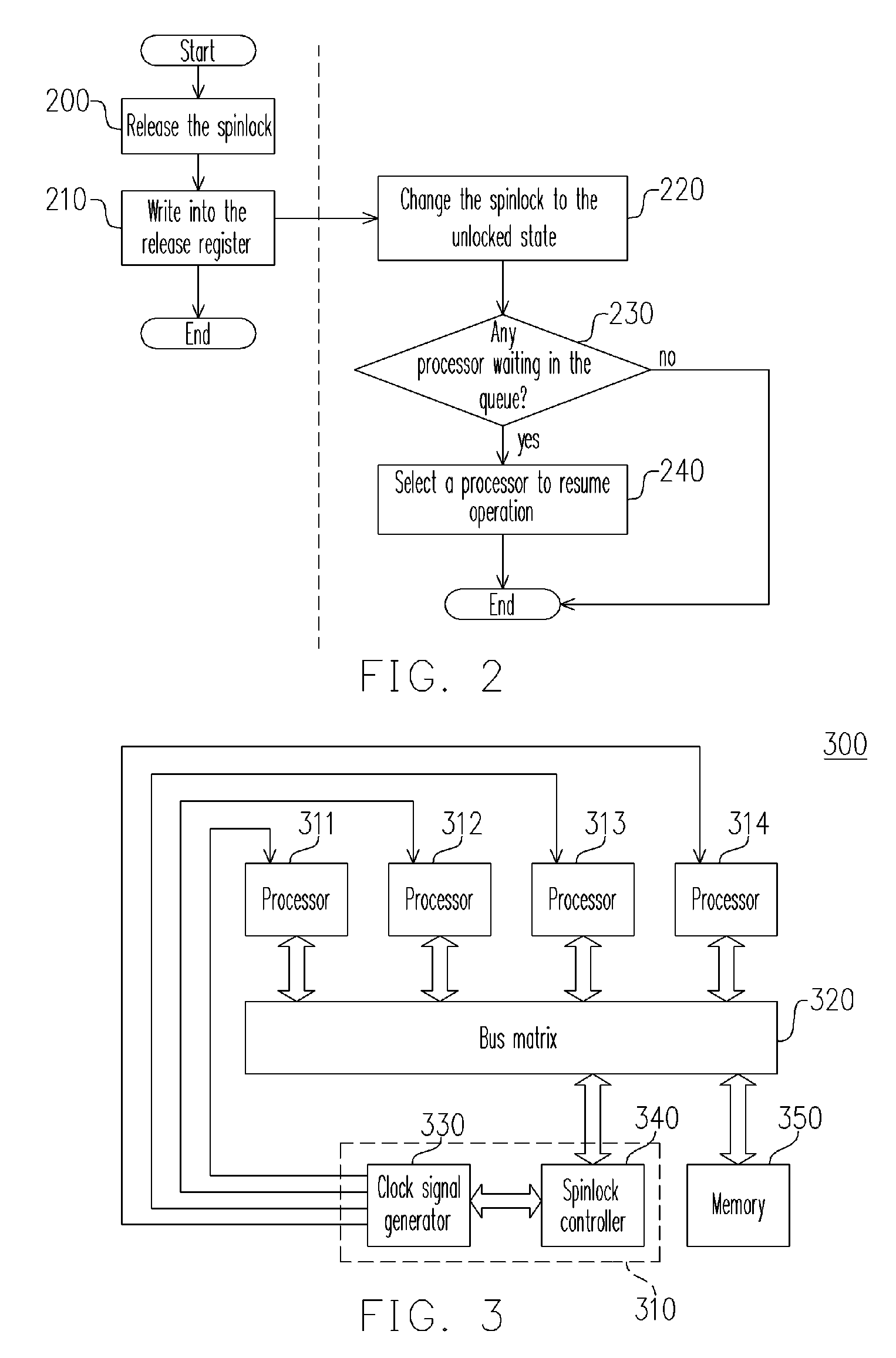
Synchronization method for a multi-processor system and the apparatus thereof
PatentInactiveUS20070050527A1
Innovation
- A synchronous method where the processor's clock signal is suspended after a failed spinlock acquisition attempt, with operations resumed only when the spinlock is successfully acquired, eliminating the need for repeated memory polling and allowing centralized spinlock management without atomic operations.

Simulation method for cam shaft speed signal during fast prototype simulation of two-stroke diesel engine
PatentActiveCN105373656A
Innovation
- Collect the crankshaft speed signal of the diesel engine through MicroAutoBox, use Simulink to create a camshaft speed signal simulation model, calculate the injection advance angle and injection time, and output the simulated camshaft speed signal to RapidProSystem to achieve synchronization of the crankshaft and camshaft signals.


Material Compatibility Standards for Spintronic Prototyping
The establishment of comprehensive material compatibility standards represents a critical foundation for successful integration of spintronics with rapid prototyping technologies. Current spintronic devices rely heavily on specific material combinations that exhibit precise magnetic, electronic, and structural properties, necessitating rigorous compatibility frameworks to ensure prototype functionality and reproducibility.
Substrate compatibility emerges as the primary consideration, where traditional silicon-based platforms must accommodate novel magnetic materials such as ferromagnetic metals, antiferromagnets, and topological insulators. The thermal expansion coefficients between substrate and spintronic layers must align within acceptable tolerances to prevent stress-induced degradation during rapid thermal cycling inherent in prototyping processes. Additionally, lattice matching requirements become particularly stringent when dealing with epitaxial growth of magnetic thin films on semiconductor substrates.
Interface engineering standards define the critical parameters governing spin injection efficiency and coherence preservation across material boundaries. These standards encompass surface preparation protocols, interlayer specifications, and contamination control measures that directly impact spin transport properties. The compatibility matrix must address potential interdiffusion effects between adjacent layers, particularly at elevated processing temperatures common in additive manufacturing techniques.
Chemical compatibility protocols address the reactivity between spintronic materials and prototyping environments, including exposure to various atmospheres, solvents, and processing chemicals. Oxidation-sensitive materials like certain Heusler alloys require inert atmosphere handling, while some topological materials demonstrate sensitivity to moisture and organic contaminants. These standards must define acceptable exposure limits and protective measures for each material class.
Mechanical compatibility standards encompass adhesion strength requirements, flexibility constraints for flexible spintronic devices, and stress tolerance specifications. The standards must account for the mechanical properties mismatch between rigid magnetic materials and potentially flexible substrates used in next-generation prototyping applications.
Thermal compatibility frameworks establish temperature cycling protocols, thermal conductivity matching requirements, and phase stability criteria across the operational temperature range. These standards ensure that rapid prototyping processes do not compromise the magnetic properties or structural integrity of spintronic components, while maintaining compatibility with standard prototyping equipment thermal profiles.
Quality Control Framework for Rapid Spintronic Fabrication
The integration of spintronics with rapid prototyping technologies necessitates a comprehensive quality control framework that addresses the unique challenges posed by accelerated fabrication processes. Traditional quality assurance methods developed for conventional semiconductor manufacturing are insufficient for spintronic devices, which rely on precise control of magnetic properties, spin coherence, and interfacial characteristics that can be significantly affected by rapid fabrication techniques.
A robust quality control framework must incorporate real-time monitoring systems capable of detecting deviations in critical spintronic parameters during the fabrication process. This includes continuous assessment of magnetic anisotropy, spin-orbit coupling strength, and interfacial exchange interactions. Advanced in-situ characterization techniques such as magneto-optical Kerr effect microscopy and spin-resolved photoemission spectroscopy should be integrated directly into rapid prototyping equipment to enable immediate feedback and process correction.
The framework should establish standardized metrics specifically tailored for spintronic device performance, including spin injection efficiency, spin diffusion length, and magnetoresistance ratios. These parameters require specialized measurement protocols that can be executed rapidly without compromising device integrity. Automated testing sequences must be developed to evaluate these characteristics within the accelerated timeline constraints of rapid prototyping workflows.
Statistical process control methodologies adapted for spintronic fabrication should incorporate machine learning algorithms capable of predicting quality outcomes based on process parameters. These predictive models can identify potential defects before they manifest, enabling proactive adjustments to fabrication conditions. The framework must also account for the stochastic nature of magnetic domain formation and spin transport phenomena that are inherent to spintronic devices.
Documentation and traceability systems within the quality control framework should capture the complete fabrication history of each prototype, including environmental conditions, material batch information, and processing parameters. This comprehensive data collection enables rapid identification of quality issues and facilitates continuous improvement of the rapid prototyping process for spintronic applications.
Unlock deeper insights with PatSnap Eureka Quick Research — get a full tech report to explore trends and direct your research. Try now!
Generate Your Research Report Instantly with AI Agent
Supercharge your innovation with PatSnap Eureka AI Agent Platform!