
Thin-film packaging structure and display device
一种薄膜封装、显示装置的技术,应用在有机半导体器件、电气元件、电固体器件等方向,能够解决IJPInk铺展性差、填充效果差等问题,达到填充效果好、铺展性好的效果
- Summary
- Abstract
- Description
- Claims
- Application Information
AI Technical Summary
Problems solved by technology
Method used
Image

Examples
Embodiment Construction
[0039] In order to make the object, technical solution and advantages of the present invention clearer, the present invention will be further described in detail below in conjunction with the accompanying drawings. Obviously, the described embodiments are only some embodiments of the present invention, rather than all embodiments . Based on the embodiments of the present invention, all other embodiments obtained by persons of ordinary skill in the art without making creative efforts belong to the protection scope of the present invention.
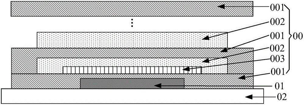
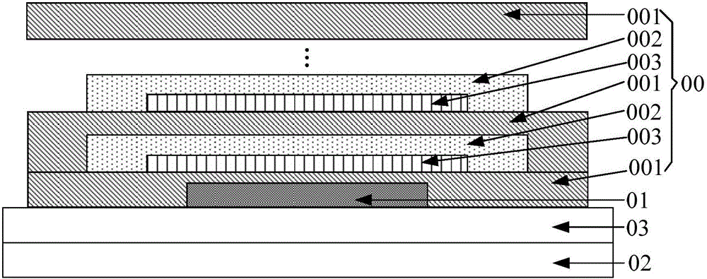
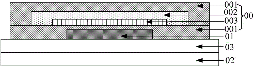
[0040] Please refer to figure 1 , which shows an application scene diagram of a thin film encapsulation structure 00 provided by an embodiment of the present invention, see figure 1 , the thin film encapsulation structure 00 includes: a plurality of film layers coated on the outside of the device to be encapsulated 01, the plurality of film layers include: alternately stacked inorganic layers 001 and organic layers 002, and among the plura...
PUM
 Abstract
Description
Claims
Application Information