Ceramic substrate manufacturing method and ceramic substrate manufactured thereby

一种陶瓷基板、制造方法的技术,应用在印刷电路制造、陶瓷层状产品、化学仪器和方法等方向,能够解决生产率降低、花费长时间、失灵等问题,达到简化制造工艺、简化蚀刻工艺、减少缺陷部分的效果

CN107889559AActive Publication Date: 2018-04-06AMOSENSE
12 Cites 7 Cited by

Patent Information

Authority / Receiving Office
CN · China
Patent Type
Applications(China)
Current Assignee / Owner
Publication Date
2018-04-06

Smart Images

  • Figure 1
    Figure 1
  • Figure 2
    Figure 2
  • Figure 3
    Figure 3
Patent Text Reader

Abstract

The present invention relates to a ceramic substrate manufacturing method and a ceramic substrate manufactured thereby, wherein a seed layer, a brazing filler layer, and a metal foil are laminated ona ceramic substrate and are brazed such that the metal foil is firmly bonded to the ceramic substrate through a brazing bonding layer, thereby substantially improving the bonding forces of the metal foil and of the ceramic substrate.
Need to check novelty before this filing date? Find Prior Art

Description

technical field

[0001] The present invention generally relates to a method of manufacturing a ceramic substrate and a ceramic substrate manufactured therefrom, and more particularly, to a method of manufacturing a ceramic substrate and a ceramic substrate manufactured therefrom, wherein the method includes firmly bonding metal foils together by brazing bonded to the ceramic substrate. Background technique

[0002] As an example of a ceramic substrate, a DBC ceramic substrate on which a metal foil (for example, copper foil) to be integrated is bonded is generally used. DBC ceramic substrates used in semiconductor power modules are advantageous not only in having higher heat dissipation characteristics than the case where leads are provided on conventional heat sinks, but also in providing semiconductor substrates with improved reliability, productivity, and uniformity. The power module aspect is also advantageous because an inspection process for the bonded state of the heat...

Examples

Embodiment Construction

[0056] Hereinafter, the present invention will be described in detail with reference to the accompanying drawings. Duplicate descriptions and descriptions of known functions and configurations considered to obscure the gist of the present invention will be omitted below. The embodiments of the present invention are intended to fully describe the present invention to those skilled in the art to which the present invention pertains. Therefore, the shapes, dimensions, etc. of components in the drawings may be exaggerated to clarify the description.

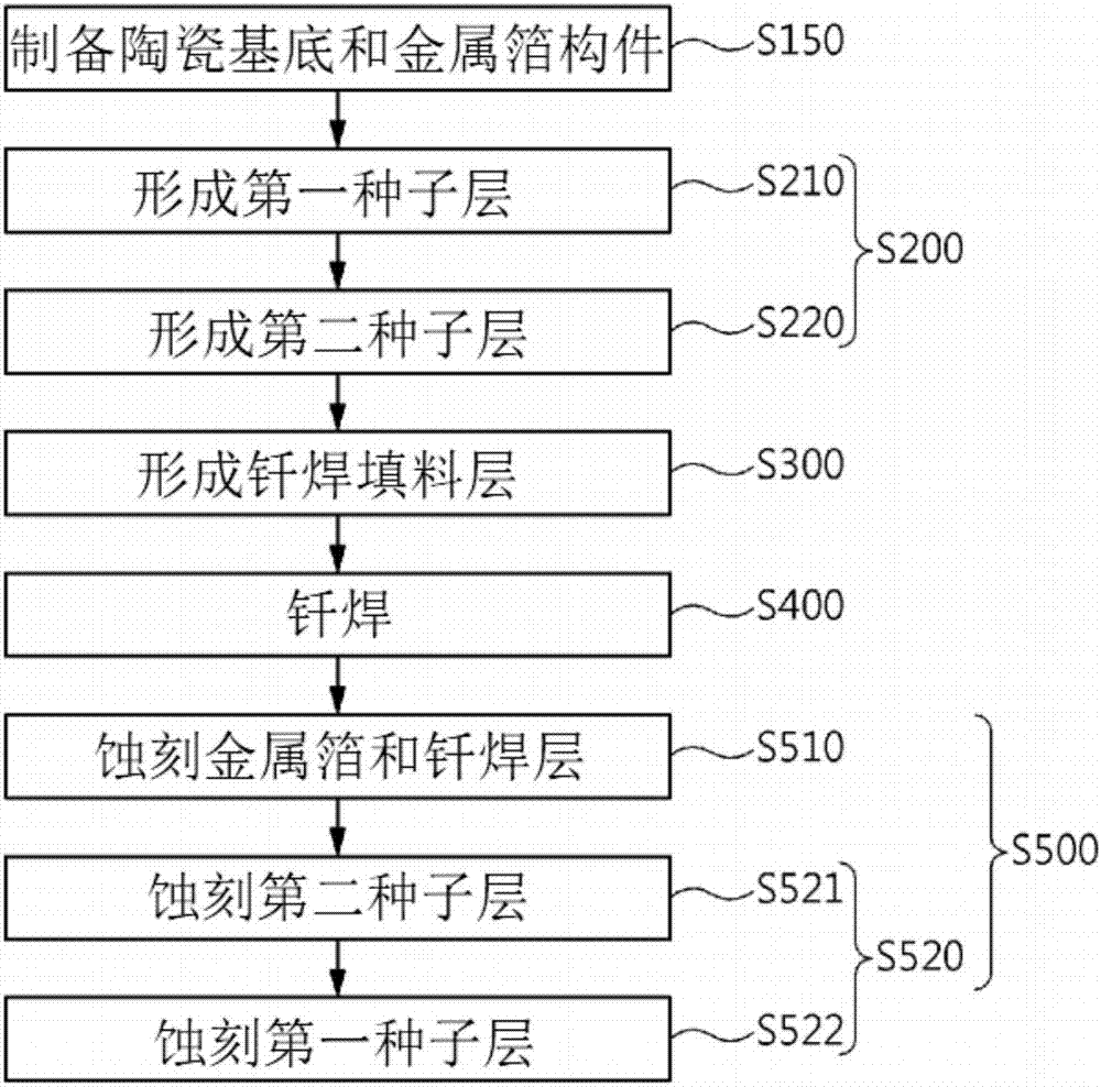
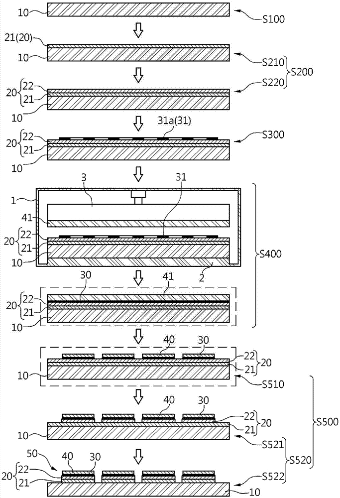
[0057] refer to figure 1 and 2 , The manufacturing method of the ceramic substrate according to one embodiment of the present invention comprises: prepare ceramic substrate 10 and metal foil 40 (S100), form seed layer 20 (S200) on ceramic substrate 10, form brazing filler on seed layer 20 layer 31 (S300), and the metal foil 40 is laminated on the brazing filler layer 31 and brazed (S400).

[0058] Preferably, preparing the cerami...