
SiC secondary epitaxial structure
A secondary epitaxy and silicon carbide technology, which is applied in the direction of electrical components, circuits, semiconductor devices, etc., can solve the problems of crystallization quality decline, device processing technology without wet etching process, and low activation rate of implanted ions
Patent Information
- Authority / Receiving Office
- CN · China
- Patent Type
- Patents(China)
- Current Assignee / Owner
- Publication Date
- 2012-02-08
Smart Images
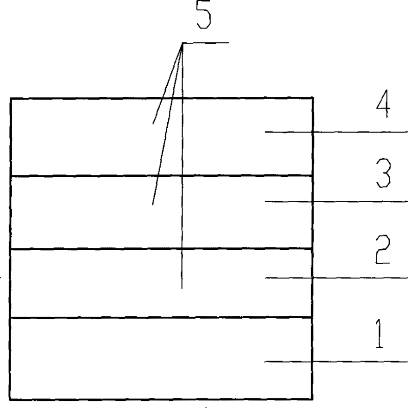
Figure 1 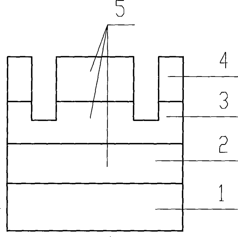
Figure 2 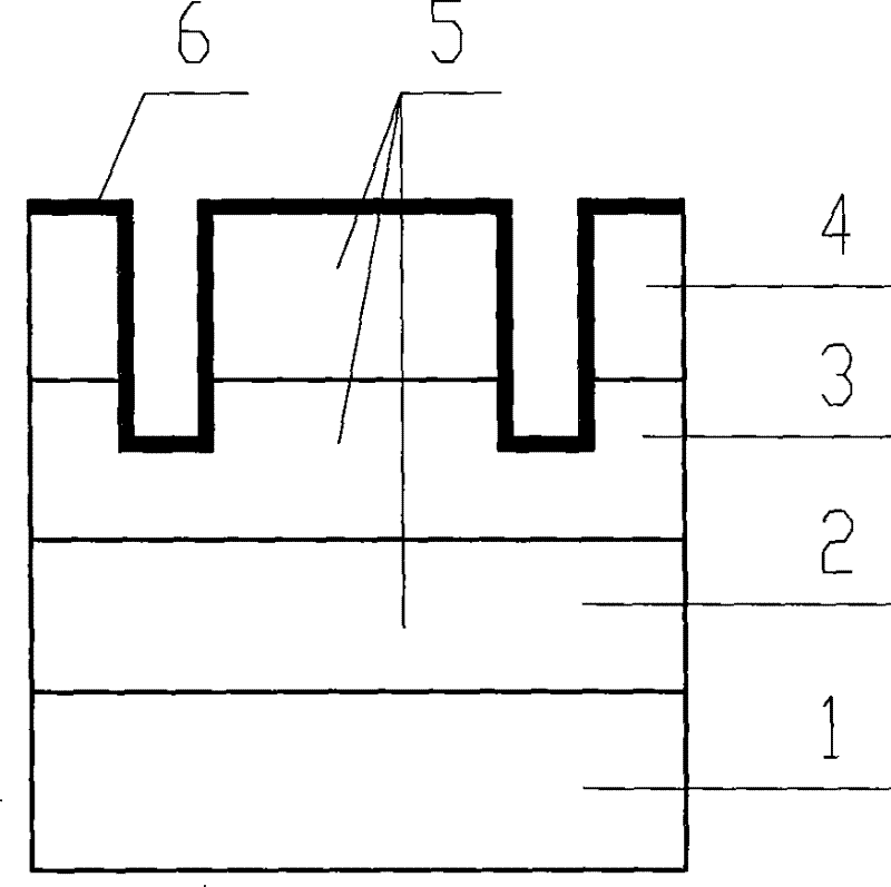
Figure 3
Abstract
Description
technical field
[0001] The invention relates to a silicon carbide secondary epitaxy structure, in particular to a silicon carbide secondary epitaxy structure which can shorten the process flow and improve the performance of silicon carbide devices. Background technique
[0002] Silicon carbide material is one of the representative materials of the third-generation semiconductor. Compared with the first-generation semiconductor element material represented by silicon and the second-generation compound semiconductor material represented by gallium arsenide, silicon carbide has a wide band gap and high critical mass. Breakdown electric field, high carrier saturation drift velocity, high thermal conductivity and other characteristics. Specifically, taking 4H-SiC as an example, at 300K (27°C), the forbidden band width of silicon carbide is 3.2eV, which is much wider than 1.12eV of silicon and 1.43eV of gallium arsenide. In this way, the operating temperature of silicon carbide m...
Examples
Embodiment Construction
[0026] The present invention will be described in further detail below in conjunction with the accompanying drawings.
[0027] Such as Figure 1-3 As shown, the silicon carbide secondary epitaxial material structure used for the preparation of silicon carbide devices includes: a silicon carbide single crystal substrate 1, a primary homoepitaxial layer 5 formed on the surface of the silicon carbide single crystal substrate 1, and a primary homoepitaxial layer The secondary epitaxial layer 6 generated on the surface of 5, the secondary epitaxial layer 6 is formed after the primary homoepitaxial layer 5 is patterned and processed, wherein the primary homoepitaxial layer 5 includes p-type silicon carbide buffer layers 2, n Type silicon carbide active layer 3 and unintentionally doped intrinsic silicon carbide layer 4 .
[0028] The invention is applicable to the preparation of the ohmic contact of the source and drain parts of the silicon carbide MESFET device. In the specific i...