
Light-receiving element and display device
A technology of light-receiving components and components, applied in the direction of electrical components, radiation control devices, electric solid devices, etc.
Patent Information
- Authority / Receiving Office
- CN · China
- Patent Type
- Patents(China)
- Current Assignee / Owner
- Publication Date
- 2011-06-01
- Estimated Expiration
- Not applicable · inactive patent
Smart Images
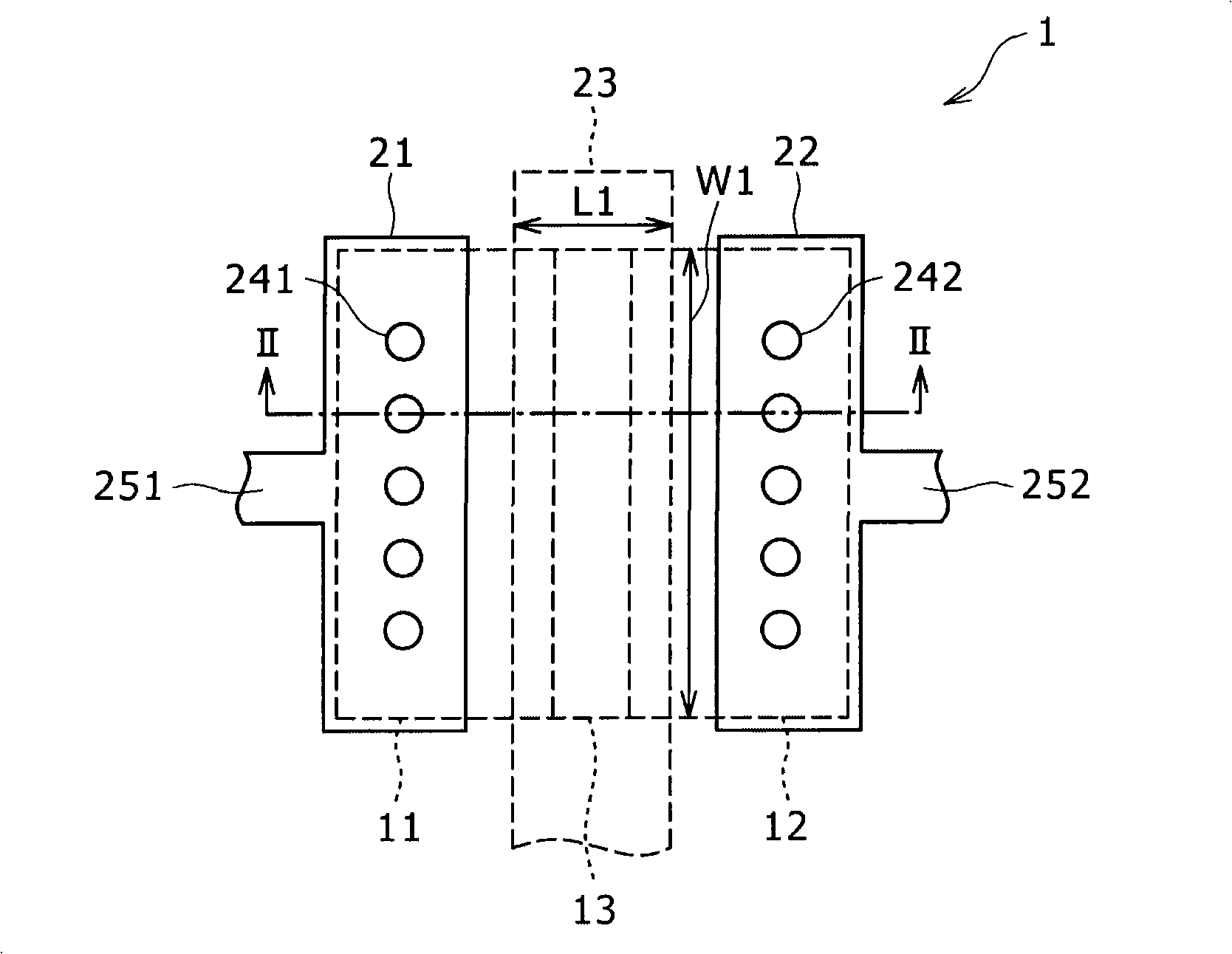
Figure 1 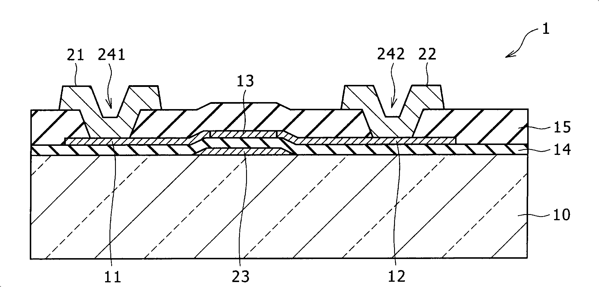
Figure 2 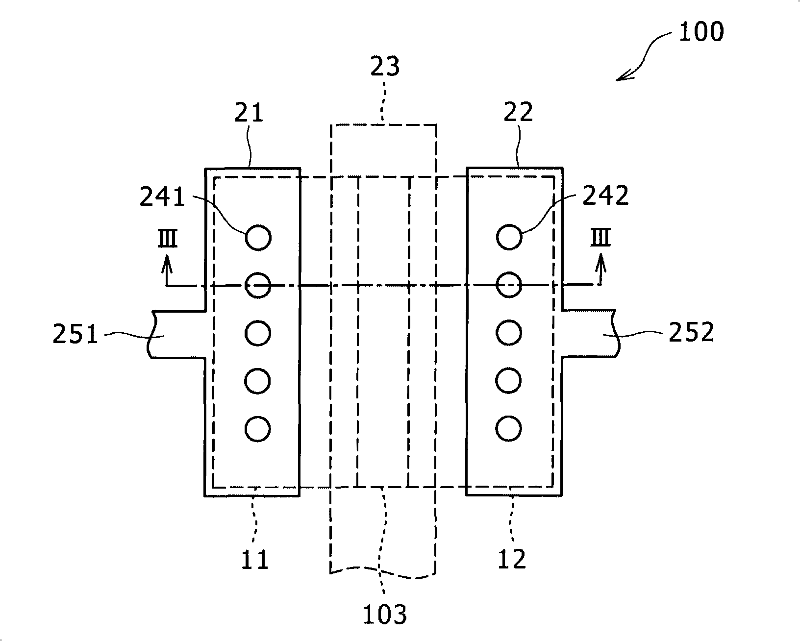
Figure 3
Abstract
Description
[0001] Cross References to Related Applications
[0002] The present invention contains subject matter related to Japanese Patent Application JP2008-228255 filed with Japan Patent Office on September 5, 2008 and Japanese Patent Application JP 2007-332100 filed with Japan Patent Office on December 25, 2007, both of which are herein The entire contents of the Japanese patent application are incorporated herein by reference. technical field
[0003] The present invention relates to a light receiving element having a control electrode and a display device including such a light receiving element. Background technique
[0004] In recent years, in display devices such as liquid crystal display devices and organic electroluminescent (EL) display devices, light receiving elements such as photodiodes are widely used to detect and control the brightness and contrast of displayed images. The photodiode is arranged in a display device together with a display element having a drive circ...
Examples
Embodiment Construction
[0047] Embodiments of the present invention will be described in detail below with reference to the accompanying drawings.
[0048] Structural Example of Light Receiving Element
[0049] figure 1 The planar structure of the light receiving element (light receiving element 1 ) of the embodiment of the present invention is shown. figure 2 shows along the figure 1 The cross-sectional structure of the light receiving element 1 along the middle line II-II.
[0050] The light receiving element 1 is a light sensor having a so-called PIN photodiode. The light receiving element 1 has: a glass substrate 10; a p+ layer 11 provided on one surface side of the glass substrate 10 as a first conductivity type semiconductor region; n+ layer 12 of a type semiconductor region; and a light receiving portion 13 provided between the p+ layer 11 and n+ layer 12 as an intermediate semiconductor region. The p + layer 11 is electrically connected to the anode electrode 21 through the contact po...