
Complementary metal oxide semiconductor (CMOS) input/output interface circuit
A technology of input and output interfaces and circuits, applied in the direction of logic circuits, electrical components, pulse technology, etc., to achieve the effect of eliminating leakage current and avoiding leakage
Patent Information
- Authority / Receiving Office
- CN · China
- Patent Type
- Applications(China)
- Current Assignee / Owner
- Publication Date
- 2011-05-18
- Estimated Expiration
- Not applicable · inactive patent
Smart Images
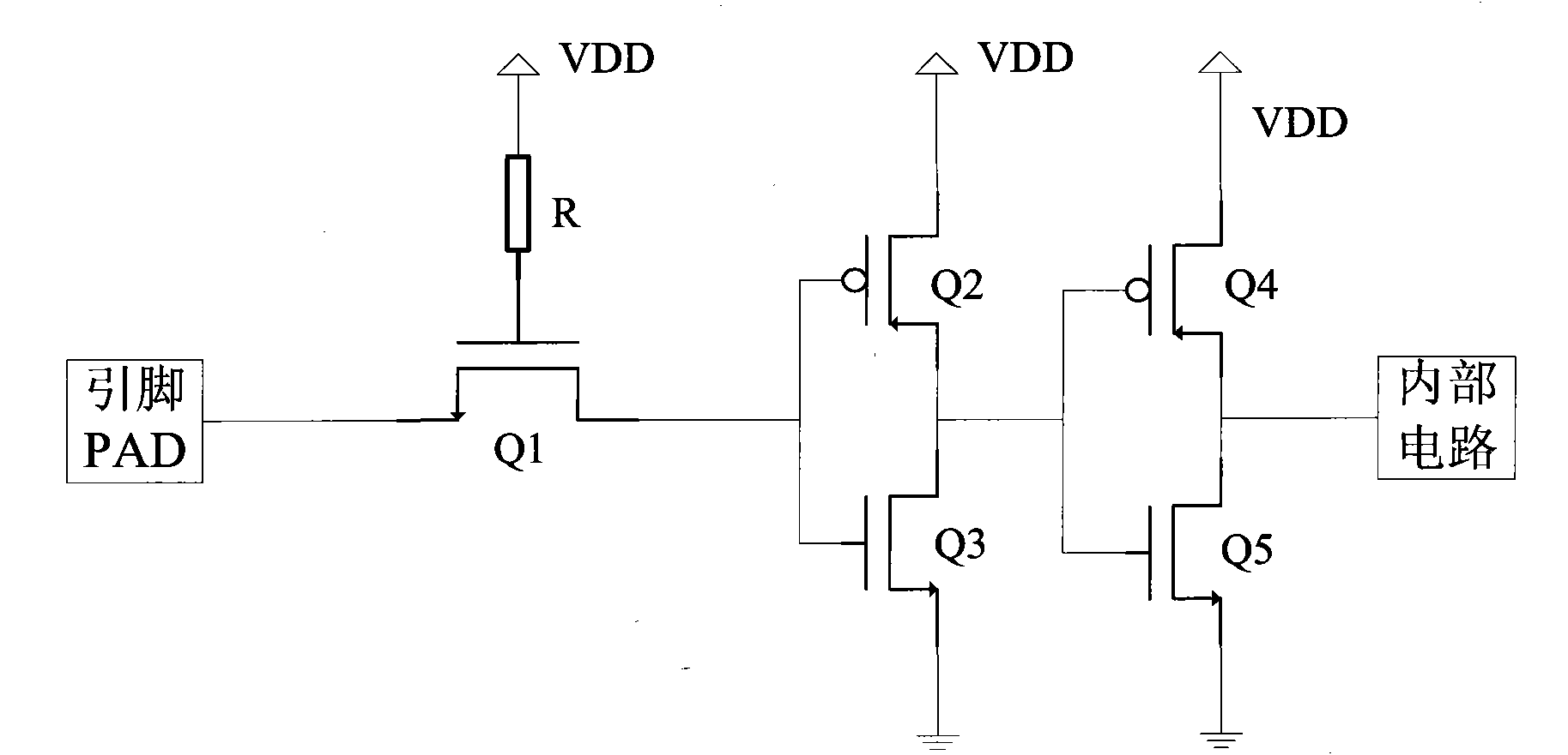
Figure 1 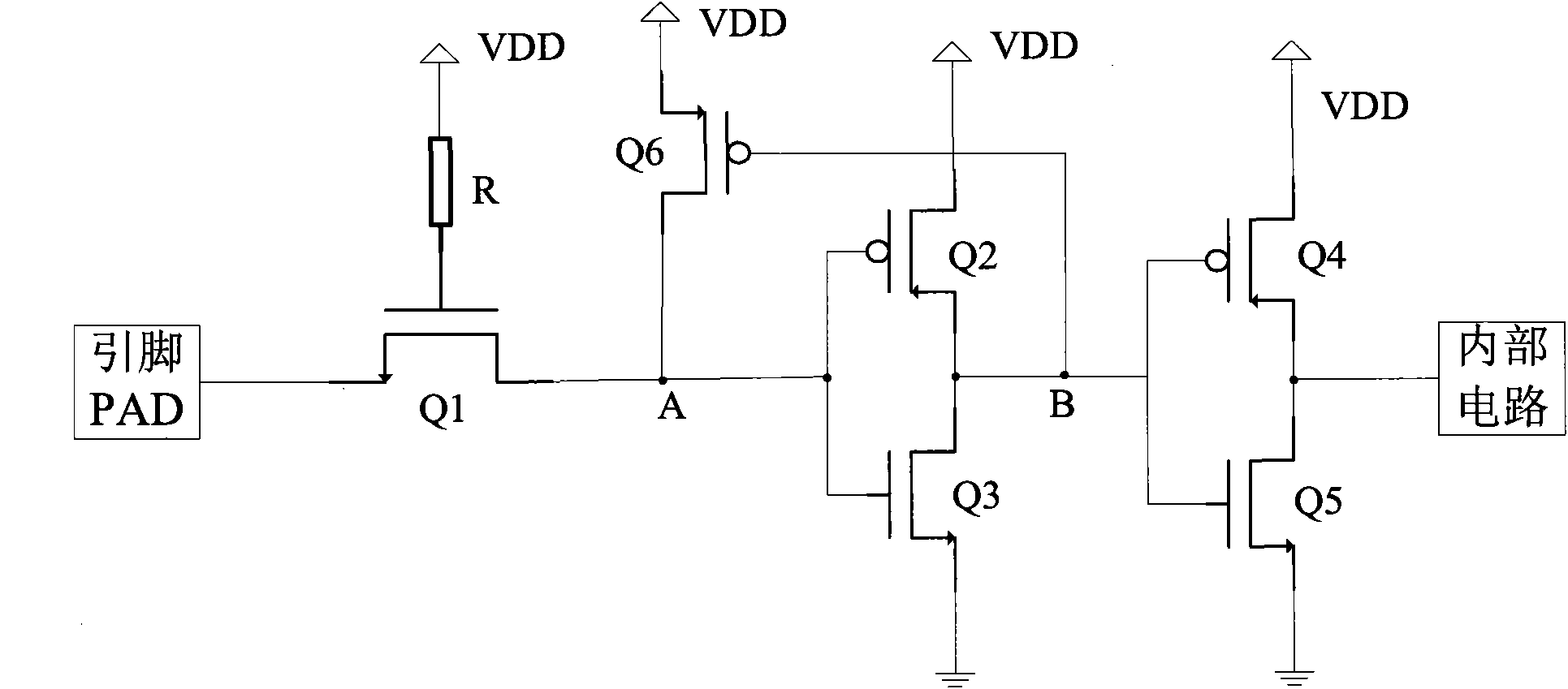
Figure 2 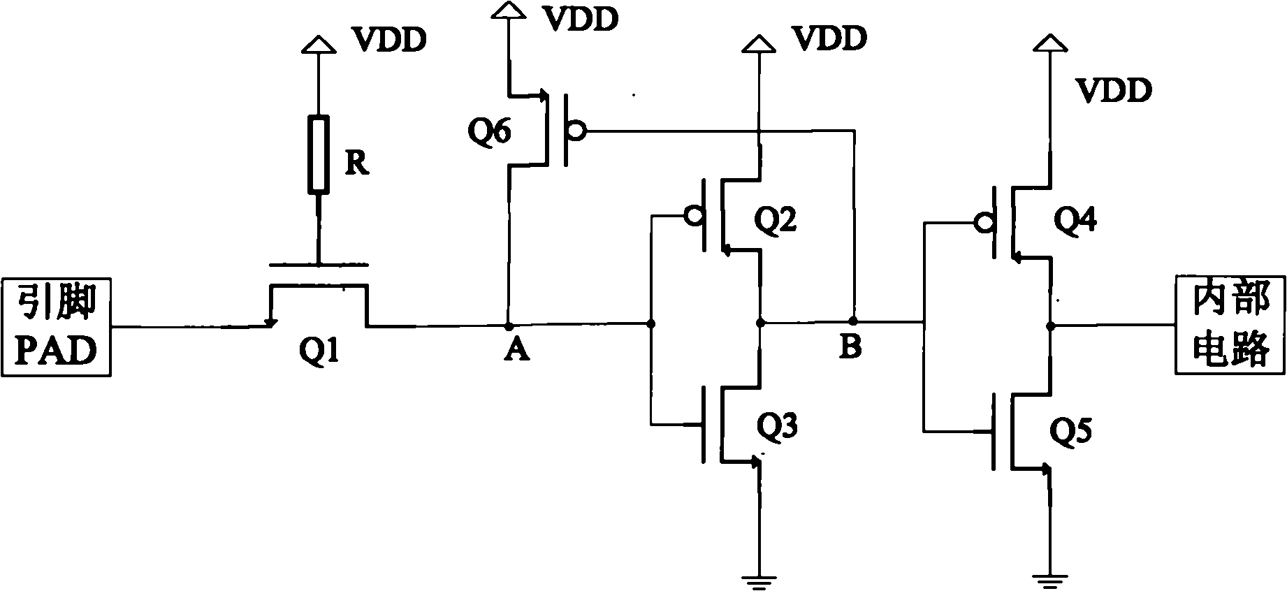
Figure 3
Abstract
Description
technical field
[0001] The invention relates to semiconductor circuit technology, in particular to a CMOS input-output interface circuit. Background technique
[0002] Typical CMOS input and output interface circuits such as figure 1 As shown, it includes a first NMOS transistor Q1, a second PMOS transistor Q2, a third NMOS transistor Q3, a fourth PMOS transistor Q2, a fifth NMOS transistor Q5, and a resistor R. The gate of the first NMOS transistor Q1 is connected to the resistor R. The power supply VDD, the source is connected to the pin, the drain is connected to the gates of the second PMOS transistor Q2 and the third NMOS transistor Q3, the drain of the second PMOS transistor Q2 is connected to the power supply VDD, the source of the third NMOS transistor Q3 is grounded, and the third NMOS transistor Q3 is connected to the ground. The source of the second PMOS transistor Q2 and the drain of the third NMOS transistor Q3 are connected to the gates of the fourth PMOS tran...
Examples
Embodiment Construction
[0011] An embodiment of the CMOS input-output interface circuit of the present invention is as figure 1 As shown, it includes a first NMOS transistor Q1, a second PMOS transistor Q2, a third NMOS transistor Q3, a fourth PMOS transistor Q4, a fifth NMOS transistor Q5, a sixth PMOS transistor Q6, and a resistor R. The first NMOS transistor Q1 The gate is connected to the power supply VDD through the resistor R, the source is connected to the pin, the drain is connected to the gates of the second PMOS transistor Q2 and the third NMOS transistor Q3, the drain of the second PMOS transistor Q2 is connected to the power supply VDD, and the third NMOS transistor Q3 The source of the second PMOS transistor Q2 and the drain of the third NMOS transistor Q3 are connected to the gates of the fourth PMOS transistor Q4 and the fifth NMOS transistor Q5, and the drain of the fourth PMOS transistor Q4 is connected to the power supply VDD. The source of the fifth NMOS transistor Q5 is grounded, ...