
Surface emitting device
A surface light-emitting element and spectrum technology, applied in electrical components, laser components, lasers, etc., can solve the problems of inability to obtain mode gain and weakening of light confinement, and achieve the effect of increasing light output and increasing mode gain
Patent Information
- Authority / Receiving Office
- CN · China
- Patent Type
- Patents(China)
- Current Assignee / Owner
- Publication Date
- 2013-03-13
Smart Images
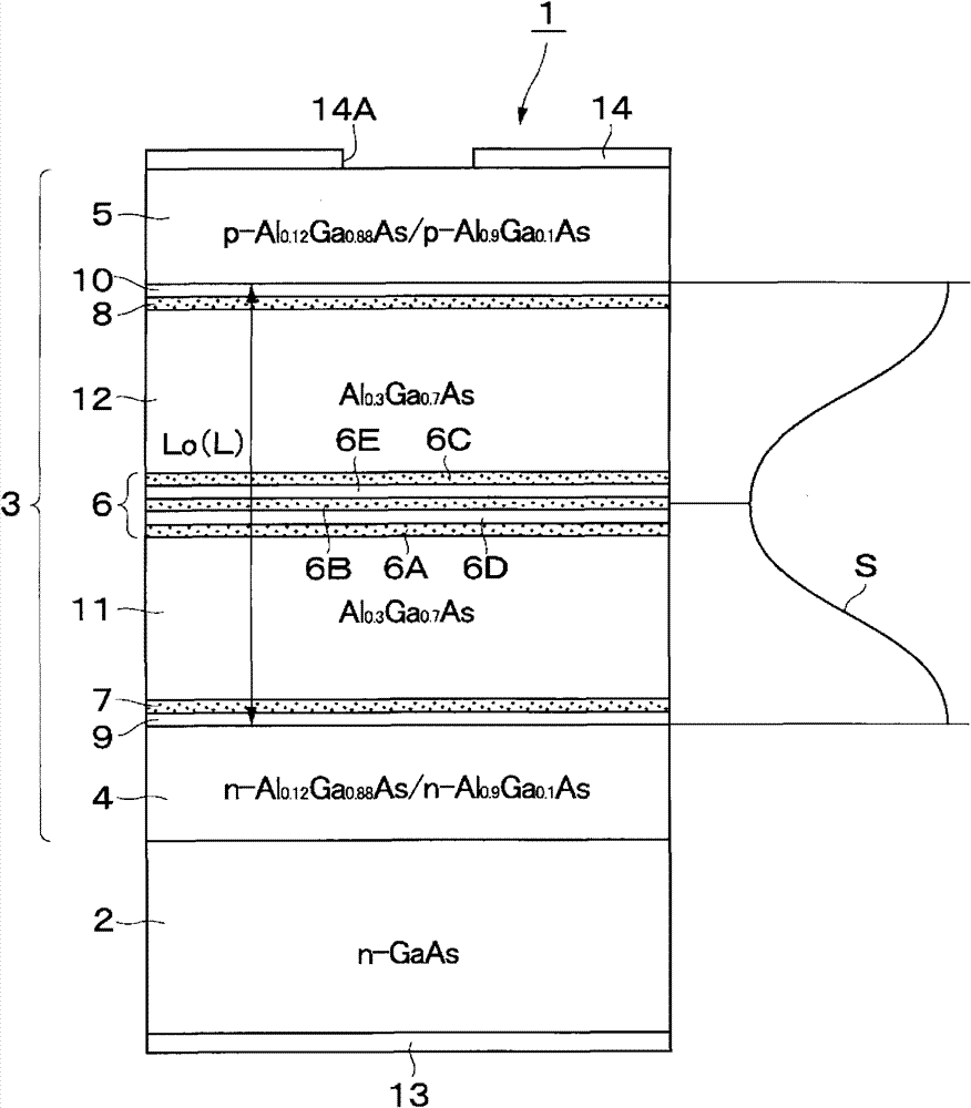
Figure 1 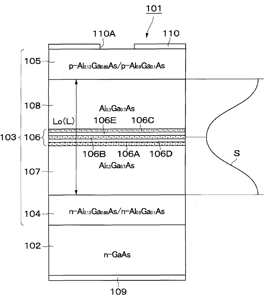
Figure 2 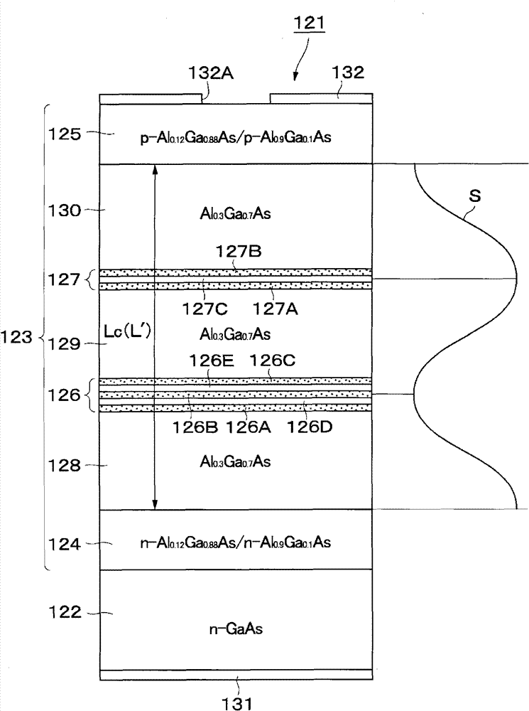
Figure 3
Abstract
Description
technical field
[0001] The present invention relates to surface emitting elements such as light emitting diodes (LEDs), vertical cavity surface emitting lasers (VCSELs) and the like. Background technique
[0002] In general, the surface light-emitting element has a lower reflective layer of the first conductivity type, a plurality of barrier layers, and a single quantum well or multiple quantum wells formed between the barrier layers on the upper surface of the first conductivity type substrate. A stacked structure of a plurality of active layers and a second conductivity type upper reflective layer. Among them, a current narrowing layer for efficiently injecting current into the active layer is provided on either the lower reflective layer or the upper reflective layer. By forming such a configuration, an optical resonator is formed by the lower reflective layer, the plurality of barrier layers, the active layer, and the upper reflective layer. Among them, the pair of low...
Examples
Embodiment Construction
[0034] Hereinafter, as an embodiment of the present invention, a vertical cavity surface emitting laser element (hereinafter referred to as a VCSEL) will be described in detail with reference to the drawings.
[0035] First, use figure 1 , and the first embodiment will be described. The VCSEL 1 according to the first embodiment includes a lower reflective layer 4, a first barrier layer 9, a first sub active layer 7 (second active layer), a first cladding layer 11, and a main A stacked structure of active layer 6 (first active layer), second cladding layer 12 , second sub-active layer 8 (second active layer), second barrier layer 10 , and upper reflective layer 5 . The lower reflective layer 4, the first barrier layer 9, the first sub-active layer 7, the first cladding layer 11, the main active layer 6, the second cladding layer 12, the second sub-active layer 8, and the second barrier layer 10 and the upper reflective layer 5, forming an optical resonator 3. However, a curr...