
High-speed full-difference clock duty cycle calibration circuit
一种校准电路、占空比的技术,应用在电气元件、产生电脉冲、脉冲处理等方向,能够解决不获得校准结果、校准精度离散性、工作的速度不能太高等问题,达到提高速度、可工作频率高、工作频率范围宽的效果
Patent Information
- Authority / Receiving Office
- CN · China
- Patent Type
- Applications(China)
- Current Assignee / Owner
- Publication Date
- 2011-06-29
- Estimated Expiration
- Not applicable · inactive patent
Smart Images
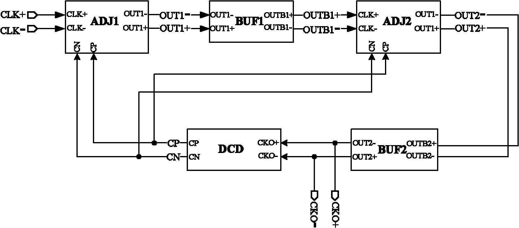
Figure 1 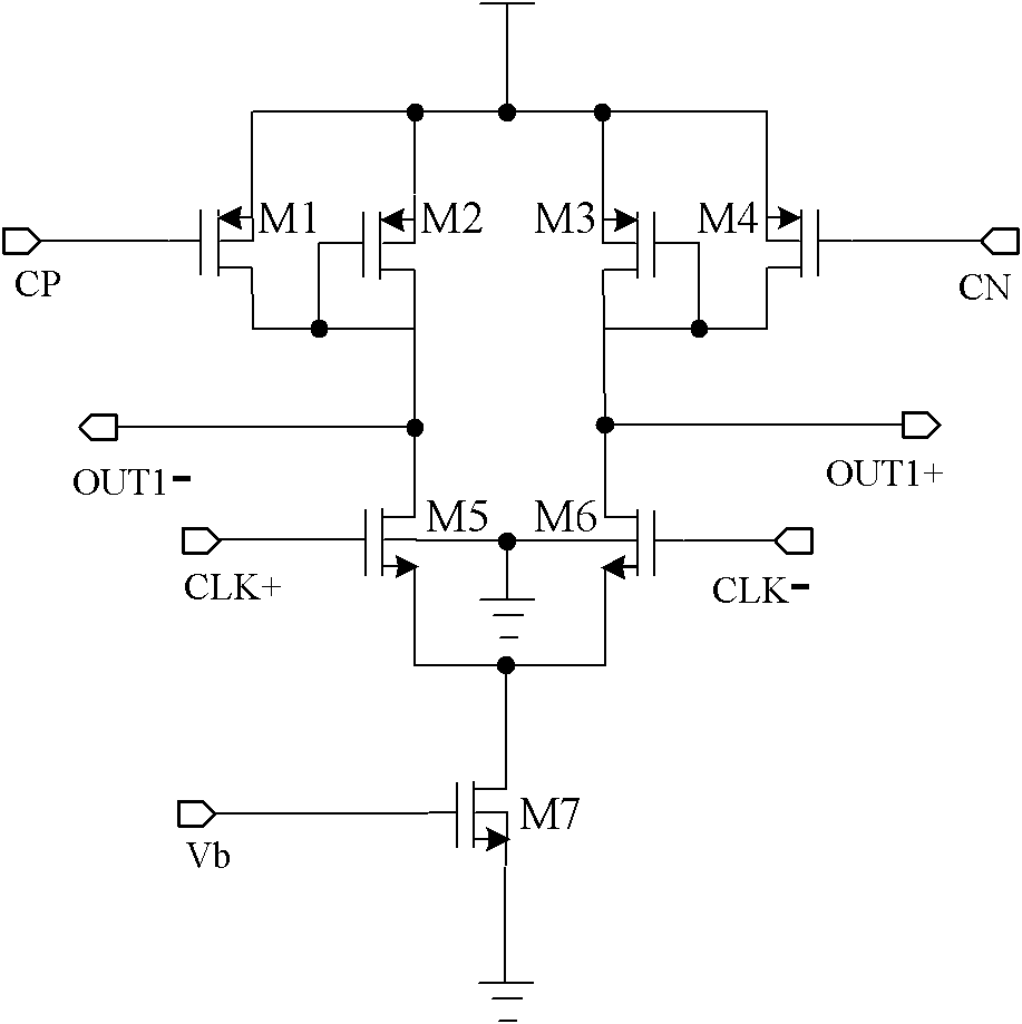
Figure 2 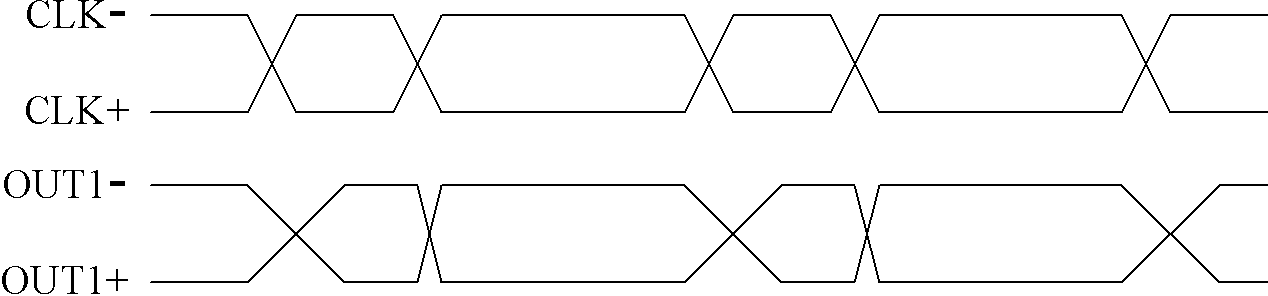
Figure 3
Abstract
Description
technical field
[0001] The invention is applicable to the application occasions of clock duty ratio calibration in various high-speed communication transmissions, such as high-speed data memory, pipeline processor, etc., and belongs to the technical field of duty ratio calibration circuit design. Background technique
[0002] With the continuous improvement of integrated circuit technology, the working speed of the chip has been continuously improved, and technologies such as double data rate (Double Data Rate, DDR), pipeline and other technologies have been widely used to obtain greater data throughput, while high-speed More stringent timing accuracy is required, which means that the performance requirements of the system clock are also stricter, and one of the important performance indicators is the duty cycle of the clock. A clock with a 50% duty cycle is most beneficial for data propagation, and for a system that adopts double data rate and pipeline operation, a 50% duty...
Examples
Embodiment Construction
[0024] The present invention will be described in detail below in conjunction with the accompanying drawings and specific examples.
[0025] The present invention calibrates the duty cycle directly on the clock chain. Such as figure 1 As shown, the input differential clocks CLK+ and CLK- are directly input to the first adjustment stage, and the duty cycle is adjusted by adjusting the rise and fall time. The output signal enters the second adjustment stage after passing through the first buffer stage. The adjustment principle is the same as that of the first adjustment stage. Similarly, the output signal is a calibrated clock signal after passing through the second buffer stage. At the same time, the output clock signal enters the duty cycle detection stage to generate control voltages CP and CN to feed back to the first and second adjustment stages to form a duty cycle calibration loop until the final output clock signal duty cycle is 50%.
[0026] Duty Cycle Adjustment
[...