
Barrier type silicon-based thin film semi-laminated solar cell
A technology of silicon-based thin film and stacked sun, which is applied in the direction of circuits, photovoltaic power generation, electrical components, etc., can solve the problems of increasing current, difficult selection of intermediate layers, and increasing spectrum absorption
Patent Information
- Authority / Receiving Office
- CN · China
- Patent Type
- Patents(China)
- Current Assignee / Owner
- Publication Date
- 2013-05-08
Smart Images
Figure 1 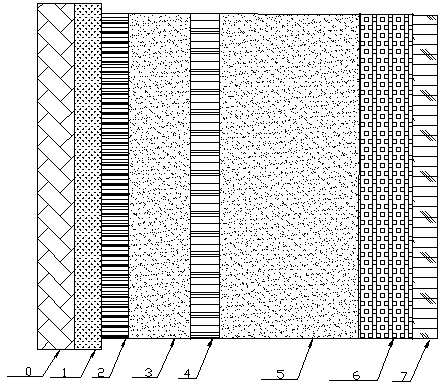
Figure 2 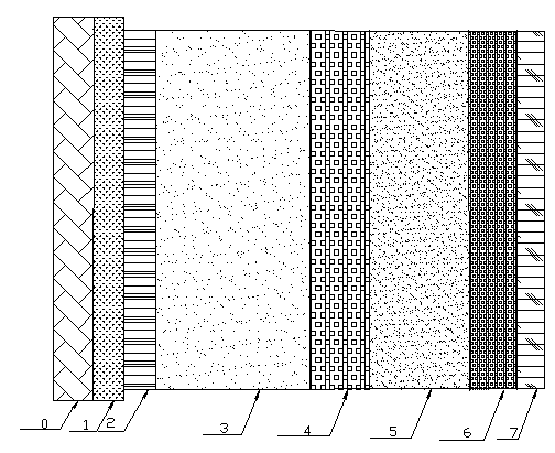
Figure 3
Abstract
Description
technical field
[0001] The invention relates to a silicon-based thin-film solar cell, in particular to a barrier-type silicon-based thin-film semi-stacked solar cell with different doping concentrations and forbidden band widths of each layer. Background technique
[0002] At present, silicon-based solar cells are mainly monocrystalline silicon, polycrystalline silicon, and thin-film silicon solar cells. Thin-film solar cells are mainly single-junction PIN structures and stacked solar cell structures. Among them, single-junction amorphous silicon cells with PIN structures Although it can absorb more solar spectrum, due to the instability of amorphous silicon, the battery has S-W effect, which limits the stability of its performance, and stacked solar cells have been greatly developed. Hydrogenated amorphous silicon cells As the top cell, the microcrystalline silicon amorphous silicon stacked cell with hydrogenated microcrystalline silicon cell as the bottom cell is a hot spo...
Examples
Embodiment Construction
[0026] 1. Structural design of solar cells
[0027] Deposition of P on a transparent glass substrate 2 I 2 P 1 I 1 N 1 and P 1 I 1 N 1 I 2 N 2 Barrier type semi-stacked thin film solar cells with structure, where P 2 I 2 P 1 I 1 N 1 and P 1 I 1 N 1 I 2 N 2 The optical bandgap Eg of each layer in the P 2 I 2 P 1 I 1 N 1 structure, P 2 The doping concentration is taken as 3.0×10 19 cm -3 , Eg=1.96eV, I 2 Eg=1.8eV, P 1 The doping concentration is 3.0×10 17 cm -3 , Eg=1.96eV, I 1 Eg=1.7eV, N 1 The doping concentration is 3.0×10 19 cm -3 , Eg=1.6eV, at P 1 I 1 N 1 I 2 N 2 structure, P 1 The doping concentration is taken as 3.0×10 19 cm -3 , Eg=1.96eV, I 1 Eg=1.8eV, N 1 The doping concentration is 3.0×10 17 cm -3 , Eg=1.75eV, I 2 Eg=1.7eV, N 2 The doping concentration is 3.0×10 19 cm -3 , Eg=1.6eV, the band gap of each layer decreases in turn, which is conducive to the full absorption of the solar spectrum, thereby improving the ...