
Gradient band gap nano-silicon thin film and graded band gap nano-silicon thin film solar cell
A nano-silicon thin film and solar cell technology, which is applied in circuits, photovoltaic power generation, electrical components, etc., can solve the problems of low open-circuit voltage and fill factor, large light-induced attenuation, and low conversion efficiency of nano-silicon solar cells, so as to avoid interface problems. effect, increased short-circuit current, and low manufacturing cost
Patent Information
- Authority / Receiving Office
- CN · China
- Patent Type
- Patents(China)
- Current Assignee / Owner
- Publication Date
- 2017-02-08
Smart Images
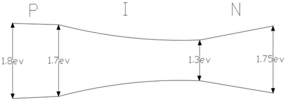
Figure 1 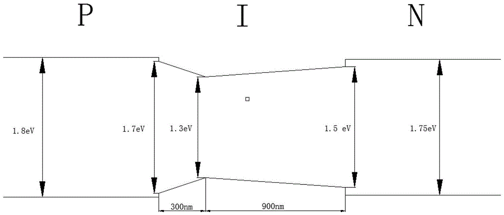
Figure 2 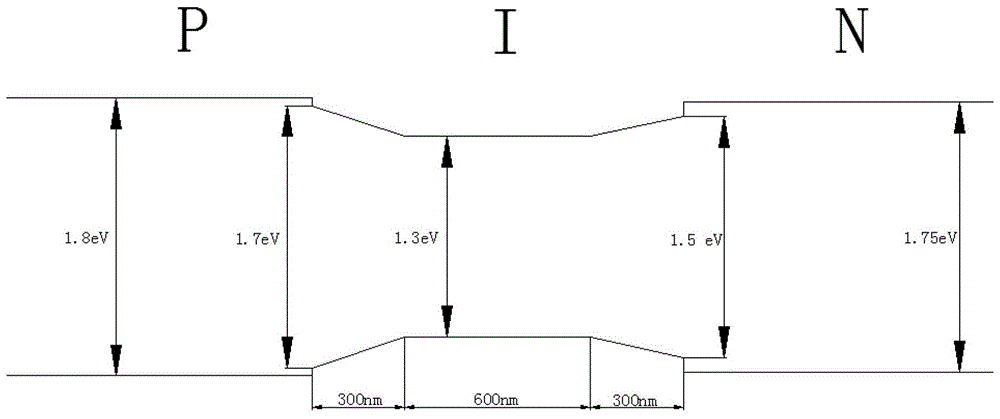
Figure 3
Abstract
Description
technical field
[0001] The invention relates to the field of silicon thin-film solar cells, in particular to a nano-silicon thin film with a gradient band gap and a solar cell made of the nano-silicon thin film. Background technique
[0002] Silicon thin-film solar cells have the advantages of less raw material consumption, easy large-area continuous production, and less pollution in the preparation process; they are an important development direction of photovoltaic cells. Amorphous silicon cells have a light-induced degradation effect, which limits its development. Nano-silicon (microcrystalline silicon) solar cells have good material order and basically no degradation, and can be combined with amorphous silicon cells to prepare stacked cells to improve Efficiency and cost reduction. Existing nano-silicon thin-film solar cells cannot fully absorb solar light energy in different bands, have low power conversion efficiency, large light-induced attenuation, and low open-circ...
Examples
Embodiment Construction
[0026] The graded bandgap nano-silicon thin film material in this specific embodiment is a mixed-phase material composed of amorphous silicon, crystal grains and grain boundaries. The band gap of the selected crystalline silicon is 1.12eV, and that of amorphous silicon is 1.75eV; the crystallization rate of nano-silicon thin film (the ratio of crystal phase to amorphous phase) ) ranges from 40% to 70%; by controlling the crystallization rate to change within the aforementioned range, the bandgap of the nano-silicon thin film with graded bandgap is 1.3eV~1.5eV. The method of controlling the crystallization rate includes adjusting the core preparation parameters of the nano-silicon thin film, such as the concentration of silane (SC), the level of the preparation power and the level of the preparation pressure, etc.
[0027] The graded bandgap has multiple structures, and the present invention proposes four schemes, the first such as figure 1 As shown in , a "C" type graded stru...