
Method of forming fin and method of forming fin field effect transistor
A fin-type field effect and transistor technology, which is applied in semiconductor devices, semiconductor/solid-state device manufacturing, electrical components, etc., can solve the problems that it is difficult for FinFET to obtain technology nodes, and the performance of transistors needs to be further improved, so as to achieve size reduction and reduction Defects, the effect of ensuring uniformity
Patent Information
- Authority / Receiving Office
- CN · China
- Patent Type
- Patents(China)
- Current Assignee / Owner
- Publication Date
- 2016-03-16
Smart Images
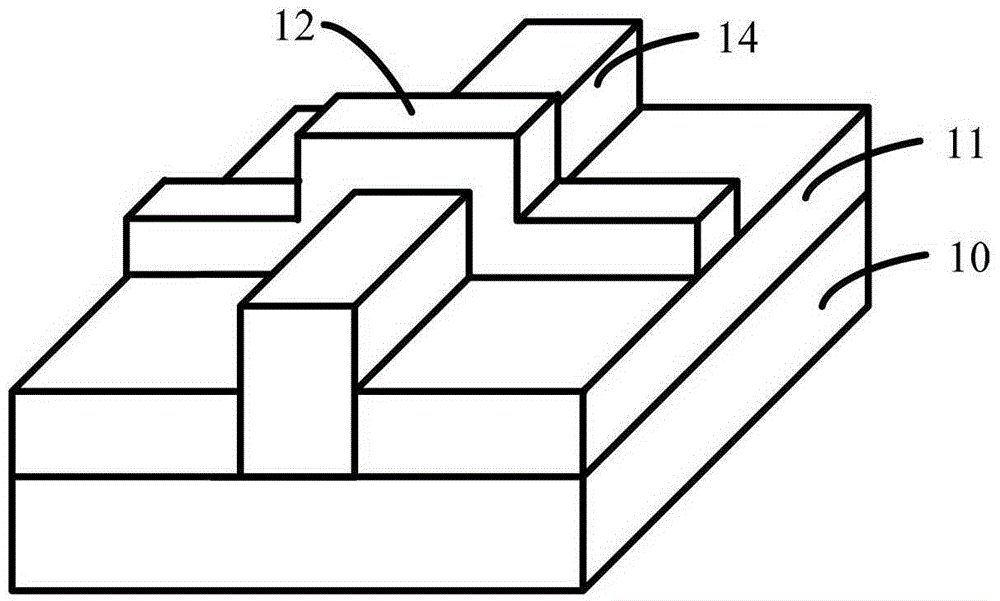
Figure 1 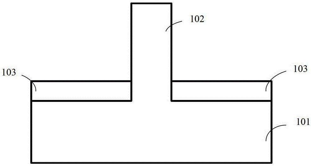
Figure 2 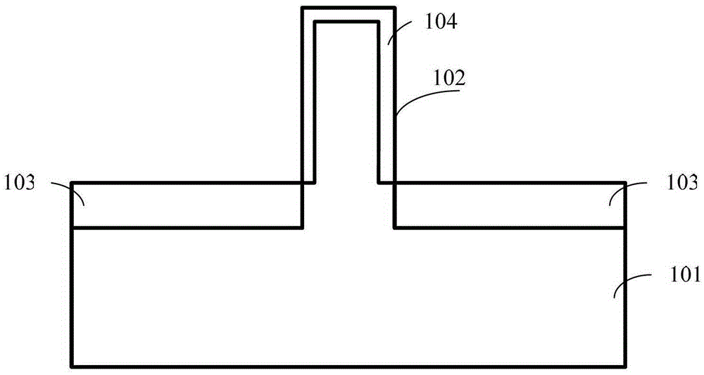
Figure 3
Abstract
Description
technical field
[0001] The invention relates to the field of semiconductor technology, in particular to a method for forming a fin and a method for forming a fin field effect transistor. Background technique
[0002] As we all know, transistors are key components in integrated circuits. In order to increase the operating speed of the transistor, it is necessary to increase the driving current of the transistor. And because the drive current of the transistor is proportional to the gate width of the transistor, to increase the drive current, the gate width needs to be increased. However, increasing the gate width conflicted with the scaling down of the semiconductor itself, leading to the development of the Fin Field Effect Transistor (FinFET).
[0003] Similar to the development of traditional two-dimensional CMOS transistors, the feature size of FinFETs is also being further reduced. It is quite difficult to manufacture FinFETs with such a small size for existing technolo...
Examples
Embodiment Construction
[0032] As mentioned in the background art, it is difficult to further reduce the technology node of the fin size by the method of forming the fin in the prior art, and the performance of the fabricated fin field effect transistor is not stable enough.
[0033] After research, it is found that it is difficult to further reduce the size of the fin portion of the FinFET due to the limitation of the existing technology such as single photolithography or etching process due to the limitation of its own technology such as photolithography resolution. Further, in the prior art, there is a gap between the fin and the gate, and there is a leakage current, which affects the performance and stability of the device.
[0034] Further studies have found that the reason for the gap between the fin and the gate is that the existing technology uses chemical etching or reactive ion etching when forming the fin to cause damage to the surface of the fin, resulting in gaps on the surface of the fin...