
Load Transient Response Enhancement Circuit for Linear Regulators
A linear voltage regulator, load transient technology, applied in the physical field, can solve the problems of not fast load transient response, system loop instability, etc., to overcome the stability of the linear voltage regulator, overcome the load transient response The effect of slower, enhanced load transient response
Patent Information
- Authority / Receiving Office
- CN · China
- Patent Type
- Patents(China)
- Current Assignee / Owner
- Publication Date
- 2018-04-17
Smart Images
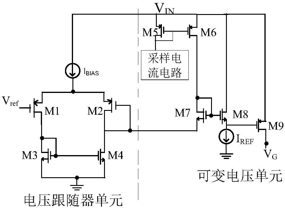
Figure 1 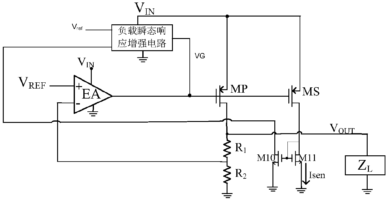
Figure 2
Abstract
Description
technical field
[0001] The invention belongs to the technical field of physics, and further relates to a load transient response enhancing circuit applied to a linear voltage regulator in the technical field of electronic circuits. The invention can be used as an important part of the linear voltage stabilizer to improve the load transient response of the linear voltage stabilizer. Background technique
[0002] With the development of integrated circuits and electronic technology, a large number of portable devices have become indispensable products in people's lives, among which linear voltage regulators are widely used due to their low cost, low noise and high precision. The load transient response is an important index of the linear voltage regulator, therefore, it is necessary to study the load transient response enhancement circuit of the linear voltage regulator.
[0003] STMicroelectronics R&D Co., Ltd. (Shenzhen) discloses a method of improving the load regulation r...
Examples
Embodiment Construction
[0016] The present invention will be further described below in conjunction with the accompanying drawings.
[0017] refer to figure 1 , the circuit structure of the present invention is described as follows.
[0018] The invention includes a voltage follower unit and a variable voltage unit.
[0019] The voltage follower unit includes a bias current device IBIAS, a first MOS transistor M1, a second MOS transistor M2,
[0020] The third MOS transistor M3 and the fourth MOS transistor M4.
[0021] The bias current I in the voltage follower unit BIAS One end of the power supply voltage V IN , the supply voltage V IN DC voltage is used, the range is 3V-6V, the other end is connected to the source of the first MOS transistor M1; the gate of the first MOS transistor M1 is connected to the reference voltage V ref , the bias voltage V ref DC voltage is used, the range is 1.4V-4V, the drain is connected to the drain of the third MOS transistor M3; the source of the second MOS t...