
Light-emitting diode micro-devices and display panels
A technology of light-emitting diodes and display panels, which is applied in semiconductor devices, electrical solid-state devices, electrical components, etc., can solve the problems of restricting the development of Micro-LEDs, low transfer efficiency, and waste of raw materials, so as to save raw materials and production costs and improve product quality. Yield rate and productivity improvement effect
Patent Information
- Authority / Receiving Office
- CN · China
- Patent Type
- Patents(China)
- Current Assignee / Owner
- Publication Date
- 2021-03-16
Smart Images
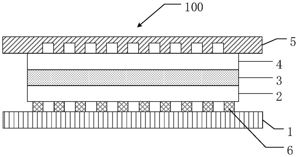
Figure 1 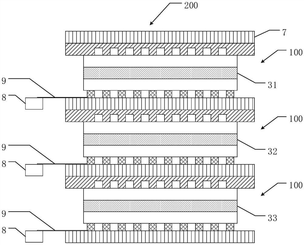
Figure 2
Abstract
Description
technical field
[0001] The invention relates to the display field, in particular to a light-emitting diode micro-device and a display panel. Background technique
[0002] Micro-LED (Micro Light-Emitting Diode, miniature light-emitting diode) technology is a popular new display device technology today. Its principle is to thin, miniaturize and array the LED structure design, and its size is only in the range of 1 to 10 meters. about. Micro-LED has many advantages. It has the advantages of high efficiency, high brightness, high reliability and fast response time of LED, and has the characteristics of self-illumination without backlight, and has the advantages of energy saving, small size and simple mechanism.
[0003] The first step of the existing Micro-LED technology is to fabricate a micron-sized light-emitting diode array on a sapphire-like substrate. The second step is to transfer the LED array to the driver board. Since the number of LED particles to be transferred is ...
Examples
Embodiment 1
[0029] Such as figure 1 As shown, this embodiment provides an LED micro-device 100 , including a light emitting chip layer 3 , a first conductive layer 2 , a second conductive layer 4 , a first transparent substrate 1 and a transparent conductive layer 5 . The first conductive layer 2 is disposed on one surface of the light emitting chip layer 3 , and the second conductive layer 4 is disposed on the other surface of the light emitting chip layer 3 . The first conductive layer 2 covers the first transparent substrate 1 . The transparent conductive layer 5 is arranged on the second conductive layer 4 and is electrically connected to the second conductive layer 4. It is an indium tin oxide semiconductor transparent conductive film (ITO conductive glass). In order to reduce the crosstalk between pixels, transparent conductive The connecting surface of the layer 5 to the second conductive layer 4 is patterned.
[0030] The light-emitting wafer layer 3 is cut from a wafer with sev...
Embodiment 2
[0034] Such as figure 2 As mentioned above, this embodiment provides a display panel 200 including a group of LED micro-devices 100 as described in Embodiment 1, and all LED micro-devices 100 in each group are stacked up and down.
[0035] Each set of LED micro-device 100 includes LED micro-device 100 with red light-emitting wafer layer 31 , LED micro-device 100 with green light-emitting wafer layer 32 and LED micro-device 100 with blue light-emitting wafer layer 33 . The LED micro-device 100 with the green light-emitting wafer layer 32 is disposed on the LED micro-device 100 with the blue light-emitting wafer layer 33 . The LED micro-device 100 with the red light-emitting wafer layer 31 is disposed on the LED micro-device 100 with the green light-emitting wafer layer 32 .
[0036] The display panel 200 provided in this embodiment further includes a second transparent substrate 7 and three driving circuits 8 . The second transparent substrate 7 is a glass substrate, which i...