
Flexible display substrate, flexible organic light emitting display device and method of manufacturing the same
a display device and organic technology, applied in the direction of organic semiconductor devices, identification means, instruments, etc., can solve the problems of brittleness and therefore prone to cracking, loss of functionality over large areas of display devices, and many parts of flexible display devices still face stability problems
Patent Information
- Authority / Receiving Office
- US · United States
- Patent Type
- Applications(United States)
- Current Assignee / Owner
- Publication Date
- 2014-08-07
Smart Images
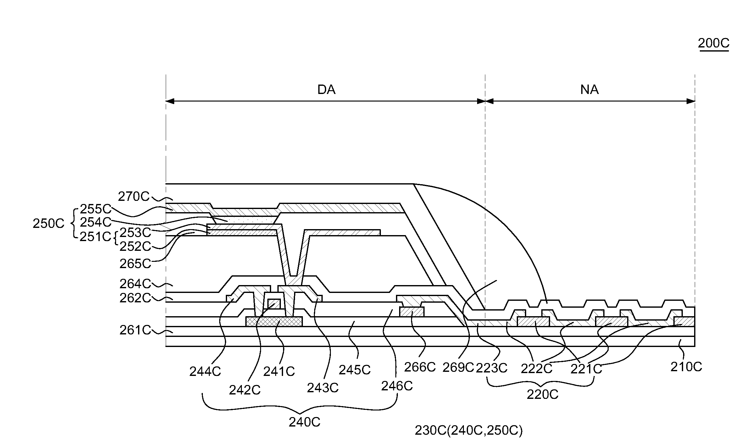
Figure 1 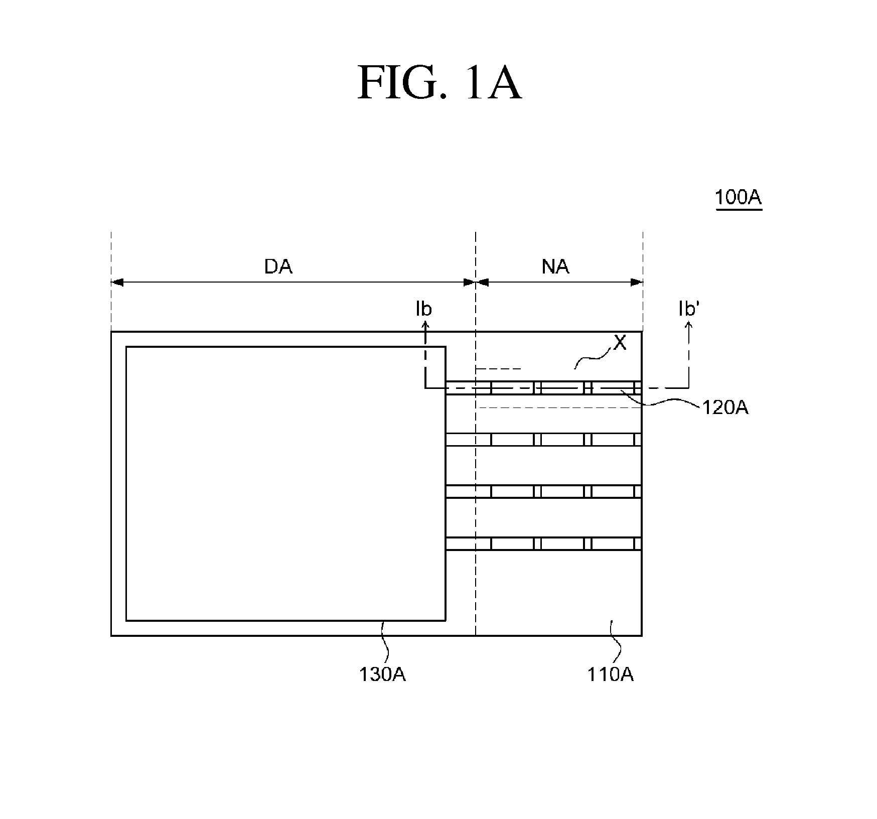
Figure 2 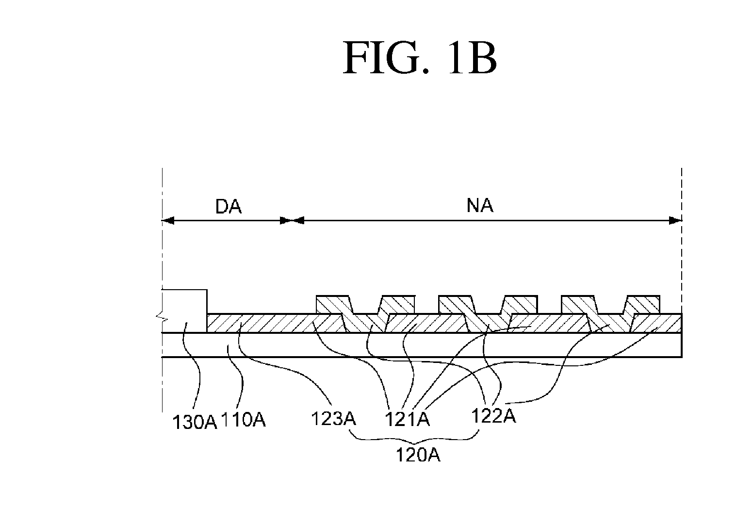
Figure 3
Abstract
Description
CROSS-REFERENCE TO RELATED APPLICATION
[0001] This application claims priority to and the benefit of Korean Patent Application No. 2013-0012032, filed on Feb. 1, 2013, the disclosure of which is incorporated herein by reference in its entirety.BACKGROUND
[0002] 1. Field of the Invention
[0003] The present invention relates to a flexible display device, and more particularly, to a flexible display substrate used in a flexible display device capable of relieving stress concentrating on a wire upon bending a substrate.
[0004] 2. Discussion of Related Art
[0005] Display devices used in monitors of computers, televisions (TVs), and cell phones include organic light emitting display devices (OLEDs) and plasma display panels (PDPs), both of which autonomously emit light, and liquid crystal display devices (LCDs) requiring a separate light source, etc.
[0006] Recently, flexible display devices capable of being bent or curved have gained much attention as the next-generation display device. Flexible dis...
Examples
Embodiment Construction
[0044]Exemplary embodiments of the present invention will be described in detail below with reference to the accompanying drawings. It is noted that the drawings of the present application are provided for illustrative purposes only and, as such, the drawings are not drawn to scale. In the following description, numerous specific details are set forth, such as particular structures, components, materials, dimensions, processing steps and techniques, in order to provide an understanding of the various embodiments of the present disclosure. However, it will be appreciated by one of ordinary skill in the art that the various embodiments of the present disclosure may be practiced without these specific details. In other instances, well-known structures or processing steps have not been described in detail in order to avoid obscuring the present disclosure.
[0045]It will be understood that when an element as a layer, region or substrate is referred to as being “on” another element, it can...