
ECP polymer additives and method for reducing overburden and defects
a technology of additives and polymer additives, applied in the field of electrochemical plating (ecp), can solve the problems of device failure or burn-in, complex interconnection of components in circuits, and subjected to precise dimensional control, so as to reduce the overburden of electroplated metals, optimize the gap filling capability, and reduce the cationic charge
Patent Information
- Authority / Receiving Office
- US · United States
- Patent Type
- Patents(United States)
- Current Assignee / Owner
- Publication Date
- 2007-02-27
- Estimated Expiration
- Not applicable · inactive patent
Smart Images
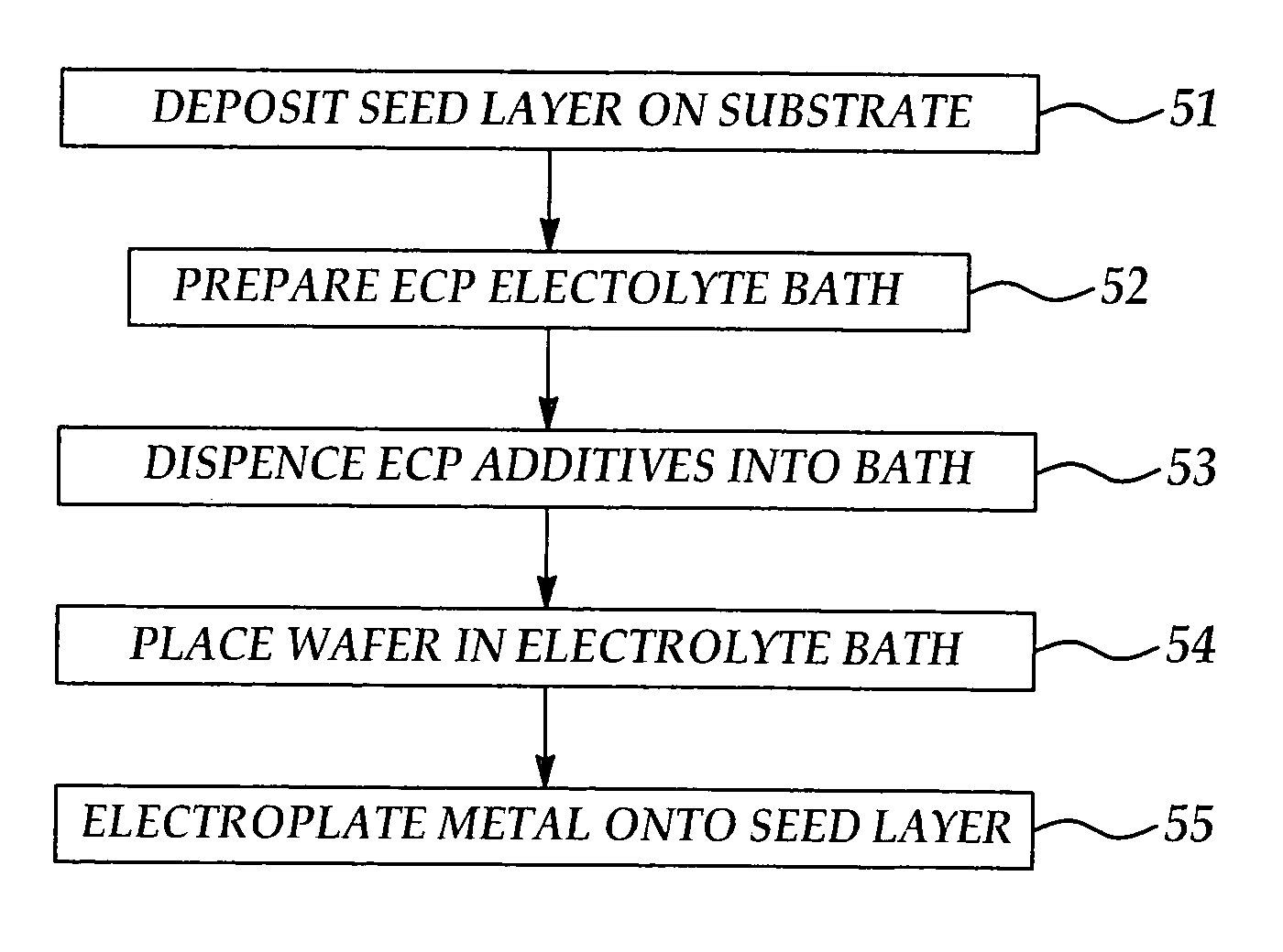
Figure 1 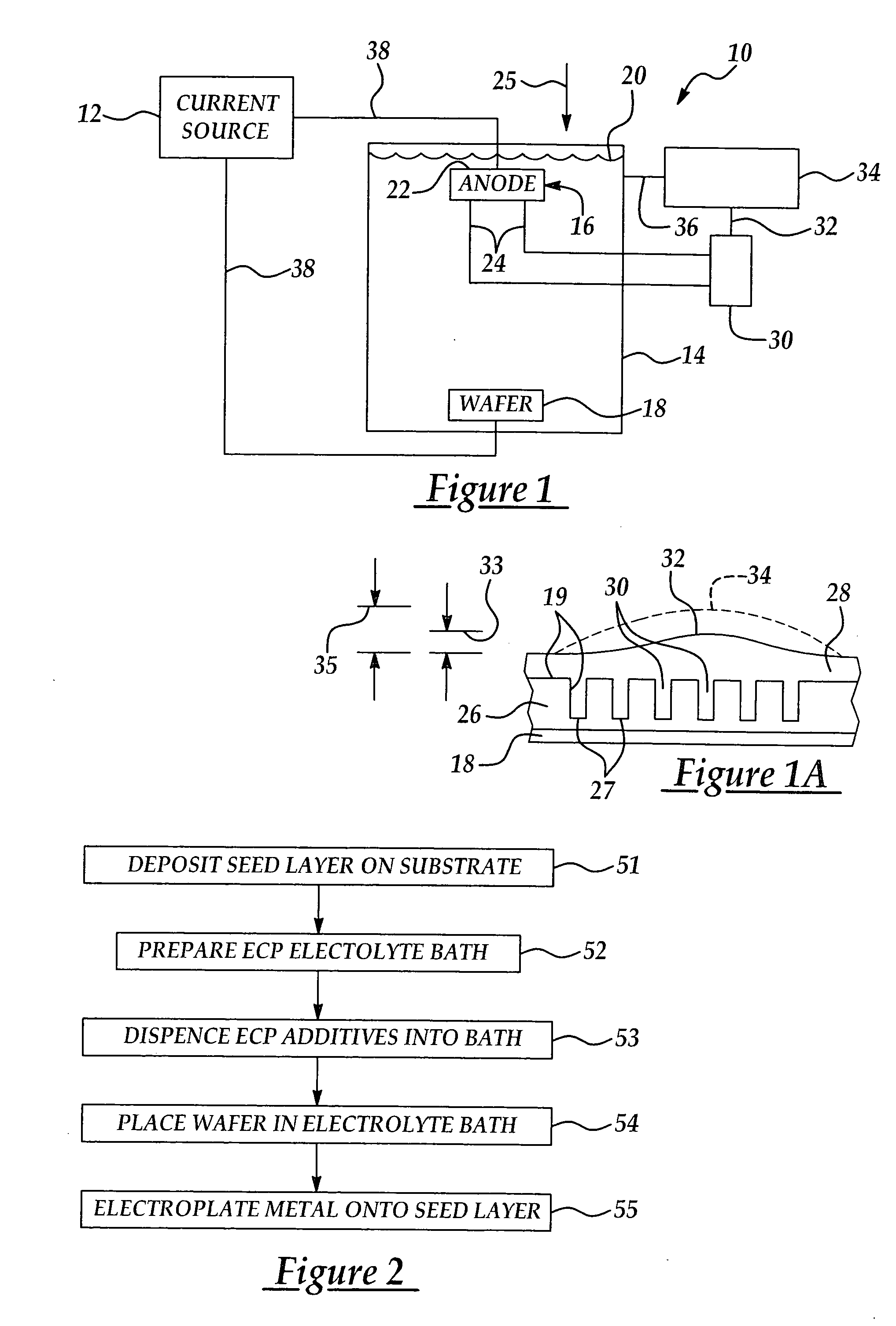
Figure 2
Abstract
Description
FIELD OF THE INVENTION
[0001] The present invention relates to electrochemical plating (ECP) processes used to deposit metal layers on semiconductor wafer substrates in the fabrication of semiconductor integrated circuits. More particularly, the present invention relates to ECP polymer additives and a method for reducing overburden and defects in the electrochemical plating of metals, particularly copper, on a substrate.BACKGROUND OF THE INVENTION
[0002] In the fabrication of semiconductor integrated circuits, metal conductor lines are used to interconnect the multiple components in device circuits on a semiconductor wafer. A general process used in the deposition of metal conductor line patterns on semiconductor wafers includes deposition of a conducting layer on the silicon wafer substrate; formation of a photoresist or other mask such as titanium oxide or silicon oxide, in the form of the desired metal conductor line pattern, using standard lithographic techniques; subjecting the waf...
Examples
Embodiment Construction
[0026]The present invention contemplates novel ECP polymer additives which reduce metal overburden in an electroplated metal while optimizing gap fill capability. Reducing the overburden on an electroplating metal reduces the quantity of metal particles generated during the subsequent chemical mechanical planarization step. Consequently, structural defects in the devices fabricated on the wafer are reduced. The polymer additives may include low cationic charge density co-polymers having aromatic and amine functional group monomers. Preferably, the low cationic charge density polymers include aromatic-functional group monomers, such as benzene or pyrollidone, aromatic amine functional group monomers, such as imidazole or imidazole derivative.
[0027]The method of the present invention includes providing an electroplating bath solution and providing low cationic charge density polymer additives in the solution. The substrate is immersed in the solution and subjected to electrochemical p...