
Liquid crystal display
a liquid crystal display and display device technology, applied in non-linear optics, instruments, optics, etc., can solve the problems of deformation of image display, affecting reliability, affecting the reliability of the system, etc., and achieve the effect of preventing the overlap of wiring at the interfa
Patent Information
- Authority / Receiving Office
- US · United States
- Patent Type
- Patents(United States)
- Current Assignee / Owner
- Publication Date
- 2009-11-03
- Estimated Expiration
- Not applicable · inactive patent
Smart Images
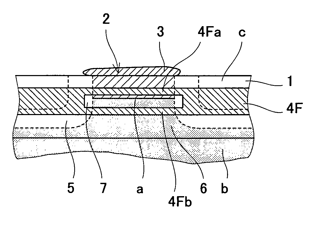
Figure 1 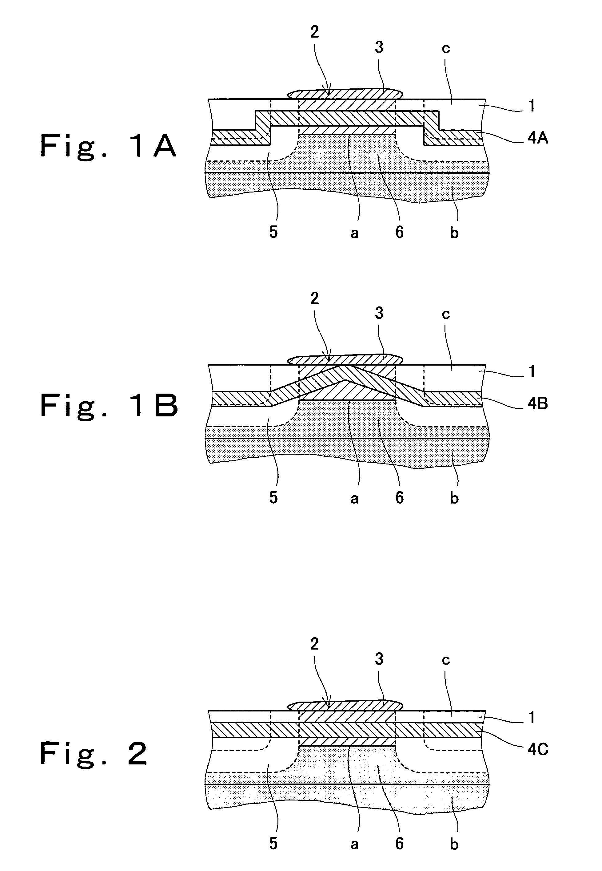
Figure 2 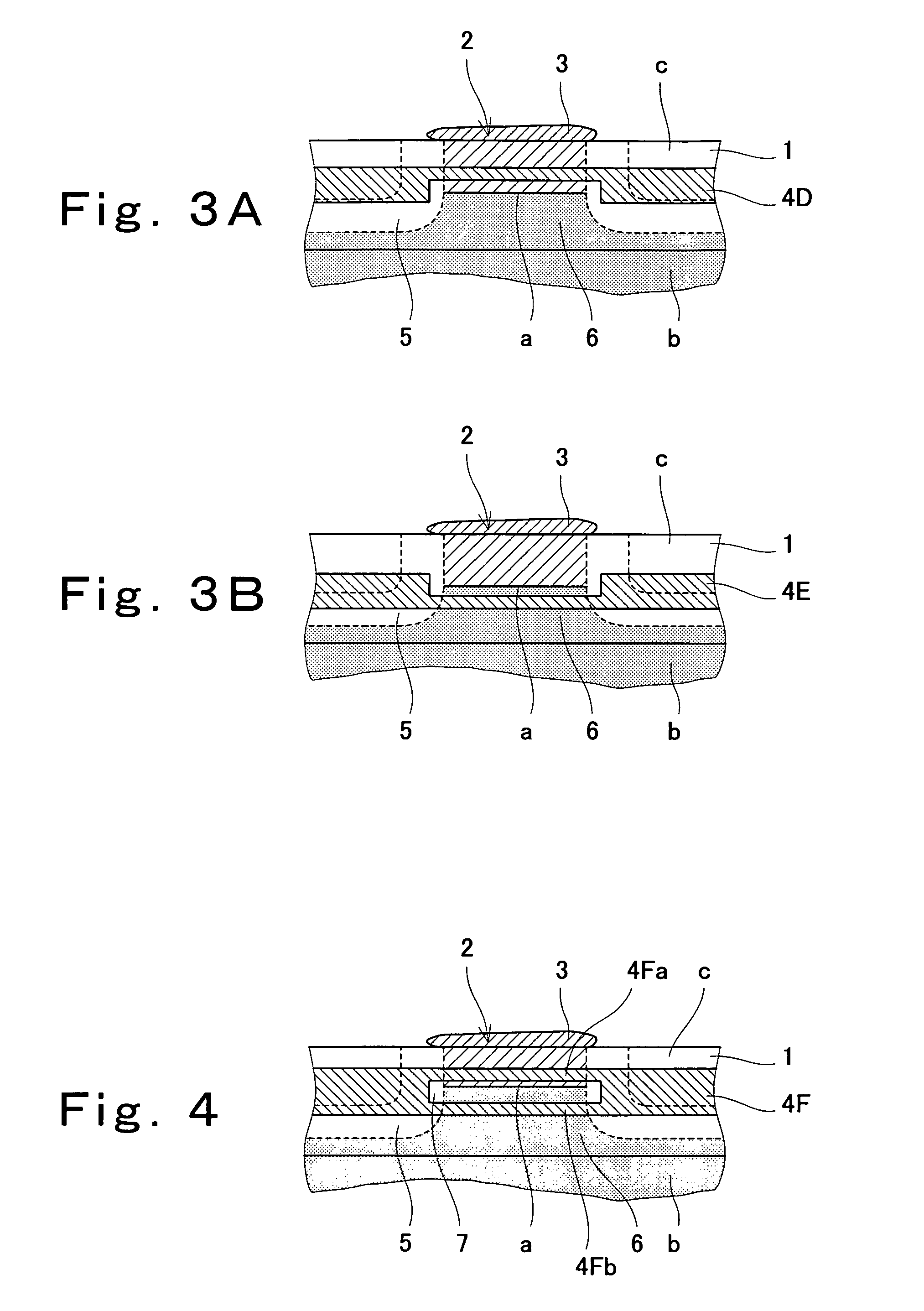
Figure 3
Abstract
Description
TECHNICAL FIELD
[0001] The present invention relates to a liquid crystal display device formed by bonding a pair of opposite substrates to each other, injecting a liquid crystal material into space between the substrates and sealing the injecting portion with an ultraviolet curing sealant.BACKGROUND ART
[0002] With the increase in display panel size for liquid crystal display devices in these years, there is a demand for a reduction in the non-display area including a bonded portion at which the substrates are bonded to each other with an adhesive or the like. For this purpose, the device design tends to narrow the spacing between the substrate peripheral edge and the display area edge (hereinafter will be referred to as “frame-narrowing”.)
[0003] FIG. 5 is a schematic plan view of the display panel of a conventional liquid crystal display device of frame-narrowing design, showing the configuration of wiring formed on a transparent substrate in the display panel. As shown in FIG. 5, the d...
Examples
embodiment 1
[0024]FIG. 1A is a schematic enlarged fragmentary plan view showing the configuration of wiring extending in a region around the liquid crystal material injecting portion of a display panel included in a liquid crystal display device according to embodiment 1 of the present invention.
[0025]As shown in FIG. 1A, the display panel of the liquid crystal display device has an arrangement in which a liquid crystal driving substrate 1 is provided with wiring 4A of a conductive metal material on an internal surface thereof and a liquid crystal material layer 6 interposed between the liquid crystal driving substrate 1 and a counter substrate positioned to face the substrate 1. The liquid crystal driving substrate 1 and the counter substrate have respective peripheral portions bonded to each other with an adhesive layer 5 except a region as a liquid crystal material injecting portion 2. The liquid crystal material layer 6 is formed to comprise a liquid crystal material injected into a clearan...
embodiment 2
[0035]FIG. 3A is a schematic enlarged fragmentary plan view showing the configuration of wiring extending in a region around the liquid crystal material injecting portion of a display panel included in a liquid crystal display device according to embodiment 2 of the present invention. Throughout FIG. 3A and FIGS. 1A and 1B, like reference characters designate like or corresponding elements.
[0036]The display panel of the liquid crystal display device according to this embodiment has the same configuration as in embodiment 1 except the following features. That is, this embodiment has wiring 4D comprising a conductive metal film, the wiring 4D being positioned not to project toward the peripheral edge of the pair of substrates in the region consisting of the liquid crystal material injecting portion 2 and the region therearound as in embodiment 1 but has a smaller line width in that region than in other region. Wiring 4D extending throughout the liquid crystal material injecting portio...
embodiment 3
[0041]FIG. 4 is a schematic enlarged fragmentary plan view showing the configuration of wiring extending in a region around the liquid crystal material injecting portion of a display panel included in a liquid crystal display device according to embodiment 3 of the present invention. Throughout FIG. 4 and FIGS. 1A and 1B, like reference characters designate like or corresponding elements.
[0042]The display panel of the liquid crystal display device according to this embodiment has the same configuration as in embodiment 1 except the following features. That is, this embodiment has wiring 4F branched to extend around the liquid crystal-sealant interface a in a region consisting of the liquid crystal material injecting portion 2 and a region therearound, thus forming detouring branch lines 4Fa and 4Fb and a rectangular opening 7 defined between these lines 4Fa and 4Fb. For the liquid crystal-sealant interface a to be located within the opening 7 in plan view, the branch line 4Fa is pos...