
Semiconductor package and fabrication method thereof
a technology of semiconductor packages and fabrication methods, applied in the direction of semiconductor devices, semiconductor/solid-state device details, electrical apparatus, etc., can solve the problems of thermal stress formed between the semiconductor package and the printed circuit board, further reduction of the package size, and degrading the quality of electrical connections, so as to reduce thermal stress, increase the amount of solder, and improve the reliability of the electronic product
Patent Information
- Authority / Receiving Office
- US · United States
- Patent Type
- Patents(United States)
- Current Assignee / Owner
- Publication Date
- 2009-12-29
Smart Images
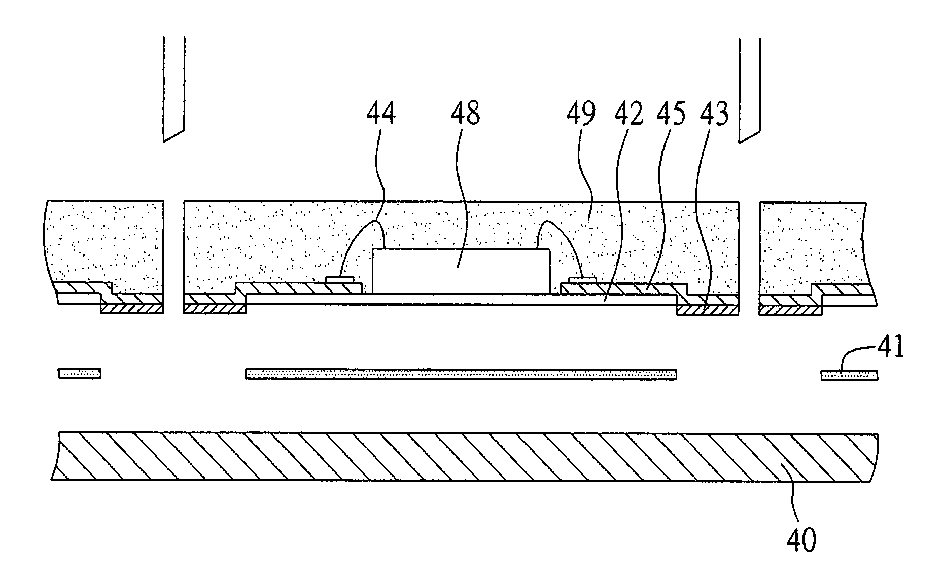
Figure 1 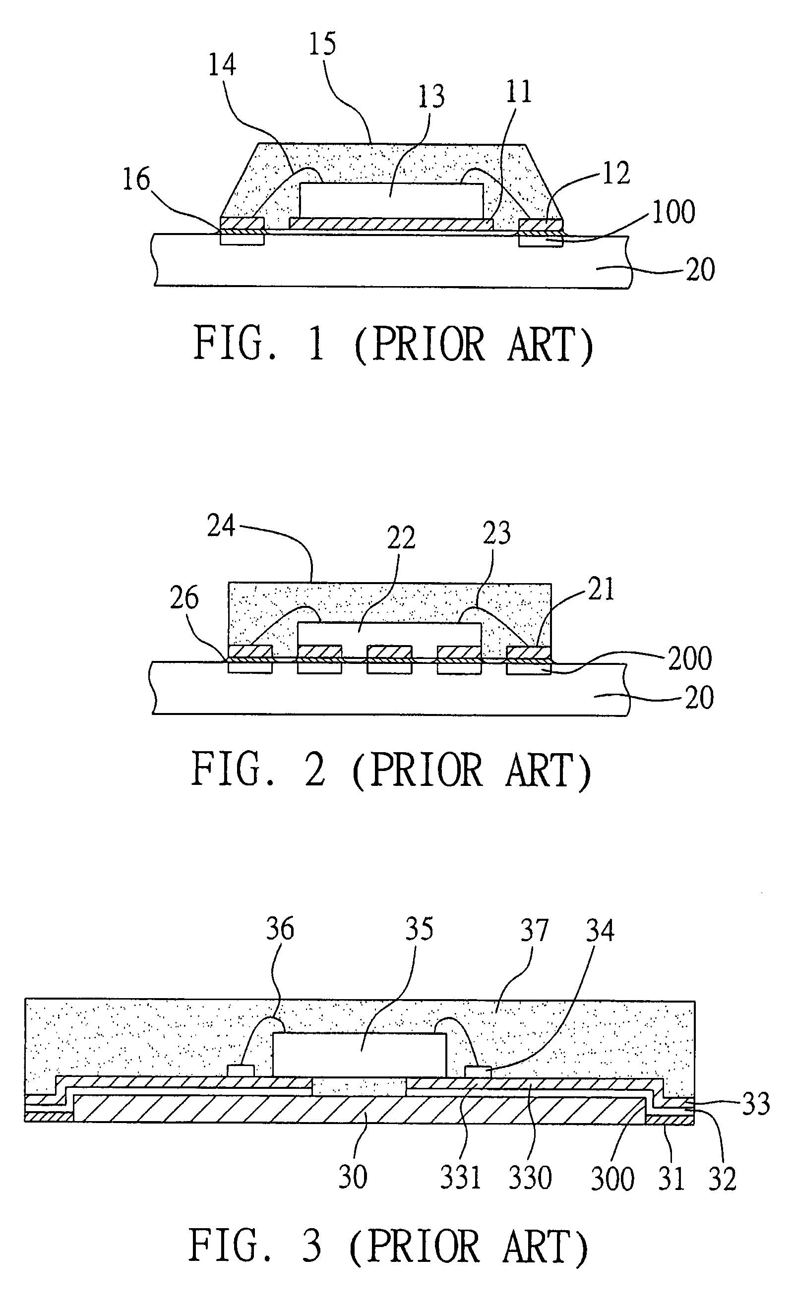
Figure 2 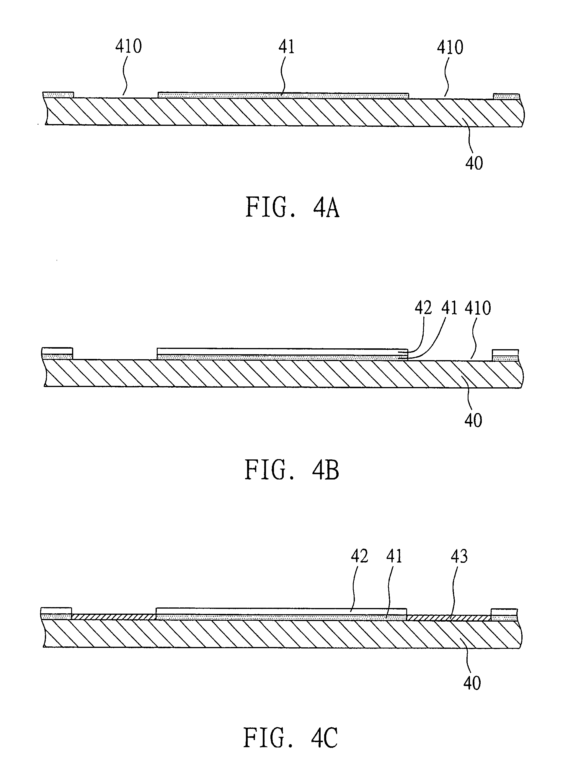
Figure 3
Abstract
Description
BACKGROUND OF THE INVENTION
[0001] 1. Field of the Invention
[0002] The present invention generally relates to semiconductor packages and fabrication methods thereof, and more particularly to a non-carrier type semiconductor package and a fabrication method thereof.
[0003] 2. Description of the Prior Art
[0004] Conventionally, a semiconductor package is often formed by using a lead frame as a chip carrier. The leadframe comprises a die pad and a plurality of leads formed around the periphery of the die pad. The lead-frame based semiconductor package is formed by attaching a semiconductor chip to the die pad and electrically connecting the semiconductor chip to the leads via the bonding wires, followed by forming an encapsulant to encapsulate the chip, die pad, bonding wires and the inner portions of the leads.
[0005] There are a great variety of lead frame based semiconductor packages, such as quad flat non-leaded (QFN) semiconductor package. The main characteristic feature of this QFN semico...
Examples
first preferred embodiment
[0029]FIGS. 4A-4G are cross-sectional views showing a semiconductor package and a fabrication method thereof according to the first preferred embodiment of the present invention.
[0030]As shown in FIG. 4A, a metal carrier 40, e.g. a copper (Cu) plate is prepared, and then a sacrificial layer 41 is applied on a surface of the metal carrier. The sacrificial layer 41 is made of, for example, polymeric material, such as epoxy resin, photo-resist, etc., and its thickness is about 10 to 30 μm. The sacrificial layer 41 has a plurality of through holes 410, formed by means of traditional photolithography, or stencil printing method.
[0031]As shown in the FIG. 4B, an insulation layer 42 is applied on the sacrificial layer 41. The insulation layer 42 is, for example, a solder mask, and is treated by photolithography to expose the through holes 410 of the sacrificial layer 41 and to further expose the metal carrier 40. Alternatively, a laser perforation process is performed on the sacrificial la...
second embodiment
The Second Embodiment
[0039]FIG. 5A and FIG. 5B are cross-sectional views illustrating a semiconductor package according to a second preferred embodiment of the present invention. As shown in FIG. 5A, the semiconductor package of the present embodiment is substantially similar to the one in the first embodiment, with only the major difference being that the chip 58 of the present embodiment is mounted on the patterned circuit layer 55 by means of flip-chip. More specifically, in the chip mounting process, the active surface of the chip 58 is facing towards the patterned circuit layer 55 to be electrically connected to the plurality of terminals 550 of the patterned circuit layer 55 or the metallic layers 56 formed on the terminals 550 via a plurality of solder bumps 54. Then, an encapsulant 59 for encapsulating the chip 58 is formed. Compared with the bonding wires that connect the chip and the patterned circuit layer, the flip-chip technology using solder bumps further shortens the ...