

Advanced Reticle Inspection Protocols for Ensuring Feature Accuracy Redesigned
MAY 20, 20269 MIN READ
Generate Your Research Report Instantly with AI Agent
PatSnap Eureka helps you evaluate technical feasibility & market potential.
Reticle Inspection Technology Background and Objectives
Reticle inspection technology has emerged as a critical component in semiconductor manufacturing, driven by the relentless pursuit of smaller feature sizes and higher device densities. As the semiconductor industry continues to push the boundaries of Moore's Law, the precision requirements for photomasks have reached unprecedented levels, necessitating advanced inspection protocols that can detect defects at the nanometer scale.
The evolution of reticle inspection began in the 1980s with basic optical inspection systems capable of detecting relatively large defects. However, as technology nodes progressed from micron-scale to sub-10nm dimensions, traditional inspection methods became inadequate. The introduction of extreme ultraviolet (EUV) lithography and the transition to 3D device architectures have further complicated the inspection landscape, requiring sophisticated detection algorithms and enhanced imaging capabilities.
Modern reticle inspection systems must address multiple challenges simultaneously, including the detection of phase defects, multilayer coating irregularities, and contamination particles that can significantly impact pattern fidelity. The complexity is amplified by the need to inspect increasingly intricate mask designs featuring optical proximity correction (OPC) patterns, sub-resolution assist features (SRAF), and complex phase-shifting structures.
The primary objective of advanced reticle inspection protocols is to ensure zero-defect manufacturing by implementing comprehensive detection strategies that encompass both printable and non-printable defects. These protocols aim to achieve defect sensitivity levels below 20nm while maintaining high throughput rates essential for volume production environments.
Contemporary inspection systems integrate multiple detection modalities, including high-resolution optical imaging, electron beam inspection, and advanced image processing algorithms powered by artificial intelligence. The convergence of these technologies enables the identification of subtle defects that could compromise wafer-level pattern accuracy and ultimately affect device performance and yield.
The strategic importance of reticle inspection extends beyond defect detection to encompass predictive maintenance, process optimization, and supply chain risk mitigation. As mask costs continue to escalate, particularly for leading-edge nodes, the economic impact of undetected defects becomes increasingly significant, making robust inspection protocols essential for sustainable semiconductor manufacturing operations.
The evolution of reticle inspection began in the 1980s with basic optical inspection systems capable of detecting relatively large defects. However, as technology nodes progressed from micron-scale to sub-10nm dimensions, traditional inspection methods became inadequate. The introduction of extreme ultraviolet (EUV) lithography and the transition to 3D device architectures have further complicated the inspection landscape, requiring sophisticated detection algorithms and enhanced imaging capabilities.
Modern reticle inspection systems must address multiple challenges simultaneously, including the detection of phase defects, multilayer coating irregularities, and contamination particles that can significantly impact pattern fidelity. The complexity is amplified by the need to inspect increasingly intricate mask designs featuring optical proximity correction (OPC) patterns, sub-resolution assist features (SRAF), and complex phase-shifting structures.
The primary objective of advanced reticle inspection protocols is to ensure zero-defect manufacturing by implementing comprehensive detection strategies that encompass both printable and non-printable defects. These protocols aim to achieve defect sensitivity levels below 20nm while maintaining high throughput rates essential for volume production environments.
Contemporary inspection systems integrate multiple detection modalities, including high-resolution optical imaging, electron beam inspection, and advanced image processing algorithms powered by artificial intelligence. The convergence of these technologies enables the identification of subtle defects that could compromise wafer-level pattern accuracy and ultimately affect device performance and yield.
The strategic importance of reticle inspection extends beyond defect detection to encompass predictive maintenance, process optimization, and supply chain risk mitigation. As mask costs continue to escalate, particularly for leading-edge nodes, the economic impact of undetected defects becomes increasingly significant, making robust inspection protocols essential for sustainable semiconductor manufacturing operations.
Market Demand for Advanced Reticle Inspection Solutions
The semiconductor industry's relentless pursuit of smaller node geometries and higher device densities has created an unprecedented demand for advanced reticle inspection solutions. As manufacturing processes approach the physical limits of lithography, the tolerance for defects on photomasks has decreased exponentially, driving the need for more sophisticated inspection protocols that can detect increasingly subtle anomalies.
The transition to extreme ultraviolet lithography and the adoption of multi-patterning techniques have fundamentally altered the inspection landscape. Traditional inspection methods that were adequate for larger feature sizes are now insufficient for detecting critical defects that could compromise yield in advanced nodes. This technological shift has created a substantial market opportunity for inspection equipment manufacturers who can deliver solutions capable of sub-nanometer defect detection with high throughput requirements.
Market drivers extend beyond pure technology advancement to encompass economic pressures within the semiconductor ecosystem. The cost of mask sets for leading-edge processes has increased dramatically, making defect-free reticles essential for maintaining acceptable return on investment. Foundries and integrated device manufacturers are increasingly willing to invest in premium inspection solutions that can prevent costly production delays and yield losses downstream.
The proliferation of artificial intelligence and machine learning applications has introduced new complexity to reticle inspection requirements. Advanced pattern recognition algorithms now demand inspection systems capable of detecting not only traditional defects but also subtle pattern variations that could impact device performance. This evolution has expanded the addressable market to include specialized inspection tools designed for specific application domains.
Geographic market dynamics reveal concentrated demand in regions with significant semiconductor manufacturing capacity. Asia-Pacific markets, particularly Taiwan, South Korea, and China, represent the largest consumption centers for advanced inspection equipment. However, emerging manufacturing hubs and the trend toward supply chain regionalization are creating new market opportunities in previously underserved territories.
The market landscape is further influenced by regulatory requirements and quality standards that mandate comprehensive inspection protocols for critical applications. Automotive, aerospace, and medical device sectors impose stringent reliability requirements that translate into demand for enhanced inspection capabilities throughout the manufacturing supply chain.
The transition to extreme ultraviolet lithography and the adoption of multi-patterning techniques have fundamentally altered the inspection landscape. Traditional inspection methods that were adequate for larger feature sizes are now insufficient for detecting critical defects that could compromise yield in advanced nodes. This technological shift has created a substantial market opportunity for inspection equipment manufacturers who can deliver solutions capable of sub-nanometer defect detection with high throughput requirements.
Market drivers extend beyond pure technology advancement to encompass economic pressures within the semiconductor ecosystem. The cost of mask sets for leading-edge processes has increased dramatically, making defect-free reticles essential for maintaining acceptable return on investment. Foundries and integrated device manufacturers are increasingly willing to invest in premium inspection solutions that can prevent costly production delays and yield losses downstream.
The proliferation of artificial intelligence and machine learning applications has introduced new complexity to reticle inspection requirements. Advanced pattern recognition algorithms now demand inspection systems capable of detecting not only traditional defects but also subtle pattern variations that could impact device performance. This evolution has expanded the addressable market to include specialized inspection tools designed for specific application domains.
Geographic market dynamics reveal concentrated demand in regions with significant semiconductor manufacturing capacity. Asia-Pacific markets, particularly Taiwan, South Korea, and China, represent the largest consumption centers for advanced inspection equipment. However, emerging manufacturing hubs and the trend toward supply chain regionalization are creating new market opportunities in previously underserved territories.
The market landscape is further influenced by regulatory requirements and quality standards that mandate comprehensive inspection protocols for critical applications. Automotive, aerospace, and medical device sectors impose stringent reliability requirements that translate into demand for enhanced inspection capabilities throughout the manufacturing supply chain.
Current State and Challenges in Reticle Feature Accuracy
The current state of reticle inspection technology represents a critical juncture in semiconductor manufacturing, where the demand for increasingly precise feature accuracy has outpaced traditional inspection capabilities. Modern reticle inspection systems primarily rely on optical and electron beam technologies, with optical systems dominating high-throughput applications and e-beam systems providing superior resolution for critical defect detection. However, these conventional approaches face significant limitations when dealing with advanced node requirements below 7nm, where feature dimensions approach the physical limits of optical wavelengths.
Contemporary inspection protocols typically employ die-to-die and die-to-database comparison methodologies, utilizing sophisticated algorithms to identify deviations in critical dimensions, pattern placement accuracy, and defect classification. Leading inspection platforms achieve detection sensitivities in the sub-10nm range for critical defects, yet struggle with nuanced pattern fidelity issues that can impact final device performance. The integration of artificial intelligence and machine learning algorithms has enhanced defect classification accuracy, but challenges remain in distinguishing between process-induced variations and genuine defects requiring correction.
The primary technical challenges encompass several interconnected domains. Resolution limitations of optical inspection systems create blind spots for detecting subtle pattern distortions and edge roughness variations that significantly impact device characteristics. Throughput constraints present another critical bottleneck, as higher resolution inspection modes dramatically increase scan times, creating manufacturing flow disruptions. The complexity of modern reticle designs, incorporating advanced optical proximity correction features and sub-resolution assist features, further complicates accurate defect identification and classification.
Pattern placement accuracy verification presents particular challenges, as current metrology capabilities struggle to achieve the sub-nanometer precision required for advanced lithography applications. The increasing prevalence of three-dimensional device architectures and complex material stacks introduces additional inspection complexities, requiring enhanced depth-of-focus capabilities and improved signal-to-noise ratios for accurate feature characterization.
Geographical distribution of advanced reticle inspection capabilities remains concentrated in key semiconductor manufacturing regions, with leading-edge facilities in Taiwan, South Korea, and select locations in the United States and Europe maintaining the most sophisticated inspection infrastructure. This concentration creates supply chain vulnerabilities and limits global access to cutting-edge inspection technologies, particularly affecting emerging semiconductor manufacturing regions seeking to establish advanced production capabilities.
Contemporary inspection protocols typically employ die-to-die and die-to-database comparison methodologies, utilizing sophisticated algorithms to identify deviations in critical dimensions, pattern placement accuracy, and defect classification. Leading inspection platforms achieve detection sensitivities in the sub-10nm range for critical defects, yet struggle with nuanced pattern fidelity issues that can impact final device performance. The integration of artificial intelligence and machine learning algorithms has enhanced defect classification accuracy, but challenges remain in distinguishing between process-induced variations and genuine defects requiring correction.
The primary technical challenges encompass several interconnected domains. Resolution limitations of optical inspection systems create blind spots for detecting subtle pattern distortions and edge roughness variations that significantly impact device characteristics. Throughput constraints present another critical bottleneck, as higher resolution inspection modes dramatically increase scan times, creating manufacturing flow disruptions. The complexity of modern reticle designs, incorporating advanced optical proximity correction features and sub-resolution assist features, further complicates accurate defect identification and classification.
Pattern placement accuracy verification presents particular challenges, as current metrology capabilities struggle to achieve the sub-nanometer precision required for advanced lithography applications. The increasing prevalence of three-dimensional device architectures and complex material stacks introduces additional inspection complexities, requiring enhanced depth-of-focus capabilities and improved signal-to-noise ratios for accurate feature characterization.
Geographical distribution of advanced reticle inspection capabilities remains concentrated in key semiconductor manufacturing regions, with leading-edge facilities in Taiwan, South Korea, and select locations in the United States and Europe maintaining the most sophisticated inspection infrastructure. This concentration creates supply chain vulnerabilities and limits global access to cutting-edge inspection technologies, particularly affecting emerging semiconductor manufacturing regions seeking to establish advanced production capabilities.
Current Advanced Reticle Inspection Protocol Solutions
01 Optical inspection systems and methods for reticle defect detection
Advanced optical inspection systems utilize high-resolution imaging and sophisticated algorithms to detect defects on reticles with enhanced accuracy. These systems employ various illumination techniques and detection methods to identify pattern irregularities, contamination, and structural defects that could affect lithographic performance.- Optical inspection systems and methods for reticle defect detection: Advanced optical inspection systems utilize sophisticated imaging techniques and algorithms to detect defects on reticles with high precision. These systems employ various illumination methods, high-resolution cameras, and image processing algorithms to identify minute defects that could affect pattern accuracy. The inspection process involves capturing detailed images of reticle patterns and comparing them against reference standards to detect anomalies, scratches, or contamination that could impact lithographic performance.
- Pattern measurement and dimensional accuracy verification: Comprehensive measurement protocols focus on verifying the dimensional accuracy of reticle patterns through precise metrology techniques. These methods involve measuring critical dimensions, line widths, spacing, and geometric features to ensure they meet specified tolerances. Advanced measurement systems use coordinate measuring techniques and statistical analysis to validate pattern fidelity and ensure manufacturing consistency across multiple reticles.
- Automated inspection algorithms and feature recognition: Sophisticated automated inspection systems employ machine learning algorithms and pattern recognition techniques to identify and classify reticle features with high accuracy. These systems can automatically detect various types of defects, measure feature dimensions, and assess pattern quality without human intervention. The algorithms are trained to recognize normal patterns and flag deviations that could affect manufacturing outcomes.
- Multi-wavelength and enhanced imaging techniques: Advanced imaging protocols utilize multiple wavelengths and specialized optical configurations to enhance defect detection capabilities and improve measurement accuracy. These techniques can reveal defects that might be invisible under standard illumination conditions and provide better contrast for accurate feature measurement. The methods often combine different optical modes to create comprehensive inspection coverage.
- Quality control standards and calibration procedures: Rigorous quality control protocols establish standardized procedures for reticle inspection, including calibration methods, reference standards, and validation techniques. These procedures ensure consistent inspection results across different systems and operators, maintaining high accuracy standards throughout the manufacturing process. The protocols include regular system calibration, performance verification, and traceability to established measurement standards.
02 Pattern matching and comparison algorithms for feature verification
Sophisticated pattern matching algorithms compare actual reticle features against reference designs to verify dimensional accuracy and pattern fidelity. These methods utilize image processing techniques to analyze critical dimensions, edge placement, and geometric characteristics of reticle patterns to ensure manufacturing specifications are met.Expand Specific Solutions03 Automated measurement and metrology systems for dimensional accuracy
Automated metrology systems provide precise measurements of reticle features including linewidth, pitch, and overlay accuracy. These systems integrate advanced measurement techniques with statistical analysis to ensure feature dimensions meet tight tolerances required for semiconductor manufacturing processes.Expand Specific Solutions04 Machine learning and AI-based inspection enhancement techniques
Artificial intelligence and machine learning algorithms enhance inspection accuracy by learning from historical defect patterns and improving detection sensitivity over time. These systems can distinguish between actual defects and false positives, reducing inspection time while maintaining high accuracy standards.Expand Specific Solutions05 Multi-wavelength and advanced illumination inspection protocols
Multi-wavelength inspection techniques and specialized illumination methods improve defect detection capabilities by revealing different types of defects that may not be visible under standard inspection conditions. These protocols optimize inspection parameters for various reticle materials and feature types to maximize detection accuracy.Expand Specific Solutions
Key Players in Reticle Inspection Equipment Industry
The advanced reticle inspection protocols market represents a mature yet rapidly evolving sector within semiconductor manufacturing, driven by increasing demand for sub-7nm process nodes and EUV lithography adoption. The market demonstrates strong growth potential, valued at several billion dollars annually, as chipmakers require enhanced defect detection capabilities for next-generation devices. Technology maturity varies significantly across players, with ASML and KLA Corp leading in cutting-edge inspection systems, while Applied Materials and D2S provide complementary mask writing and computational solutions. Asian foundries including TSMC, SMIC, and Samsung drive demand through advanced node transitions, while memory manufacturers like Micron and ChangXin Memory Technologies require specialized inspection protocols for 3D architectures. The competitive landscape shows consolidation around few key equipment suppliers serving diverse foundry and IDM customers globally.
Applied Materials, Inc.
Technical Solution: Applied Materials provides comprehensive reticle inspection solutions through their PROVision platform, incorporating advanced optical inspection with AI-driven defect detection algorithms. Their inspection protocols feature multi-wavelength illumination systems and high-numerical-aperture optics for enhanced feature resolution and defect sensitivity. The company's approach includes automated defect review and classification systems with machine learning capabilities for pattern recognition and false positive reduction. Applied Materials' inspection methodology supports both blank reticle inspection and patterned reticle verification with sub-nanometer precision measurement capabilities. Their systems integrate with fab-wide process control networks for real-time yield management and predictive maintenance scheduling.
Strengths: Comprehensive inspection portfolio, strong AI integration for defect classification, excellent fab-wide system integration capabilities. Weaknesses: Complex system configuration requirements, high operational complexity, significant training requirements for operators.
KLA Corp.
Technical Solution: KLA Corporation develops advanced reticle inspection systems utilizing high-resolution optical and e-beam technologies for critical dimension measurement and defect detection. Their inspection protocols incorporate machine learning algorithms for automated defect classification and feature accuracy verification. The company's reticle inspection solutions feature sub-10nm resolution capabilities with multi-mode inspection including brightfield, darkfield, and phase contrast imaging. Their systems integrate real-time data analytics for process control and yield optimization, enabling detection of critical defects that could impact lithographic performance. KLA's inspection protocols support advanced node requirements down to 3nm technology nodes with enhanced sensitivity for detecting pattern fidelity issues.
Strengths: Industry-leading inspection resolution and sensitivity, comprehensive defect classification capabilities, strong integration with fab process control systems. Weaknesses: High equipment costs, complex system maintenance requirements, lengthy inspection cycle times for comprehensive analysis.
Core Innovations in Feature Accuracy Detection Methods
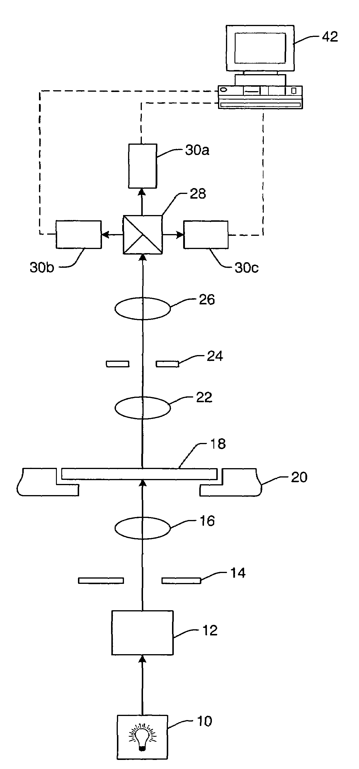
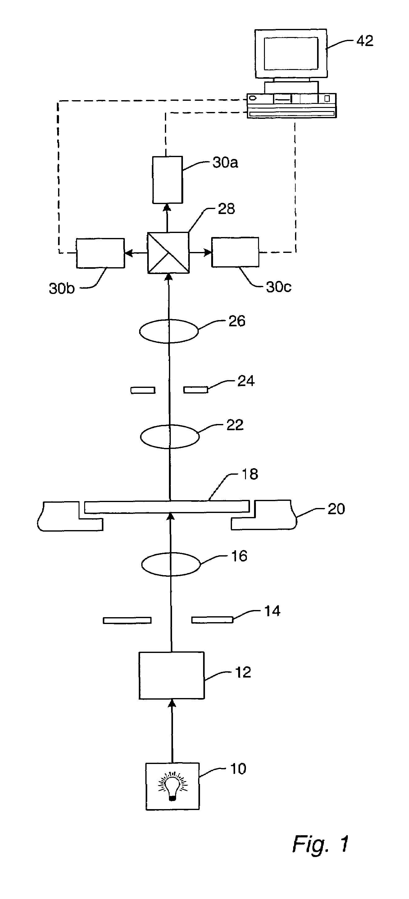
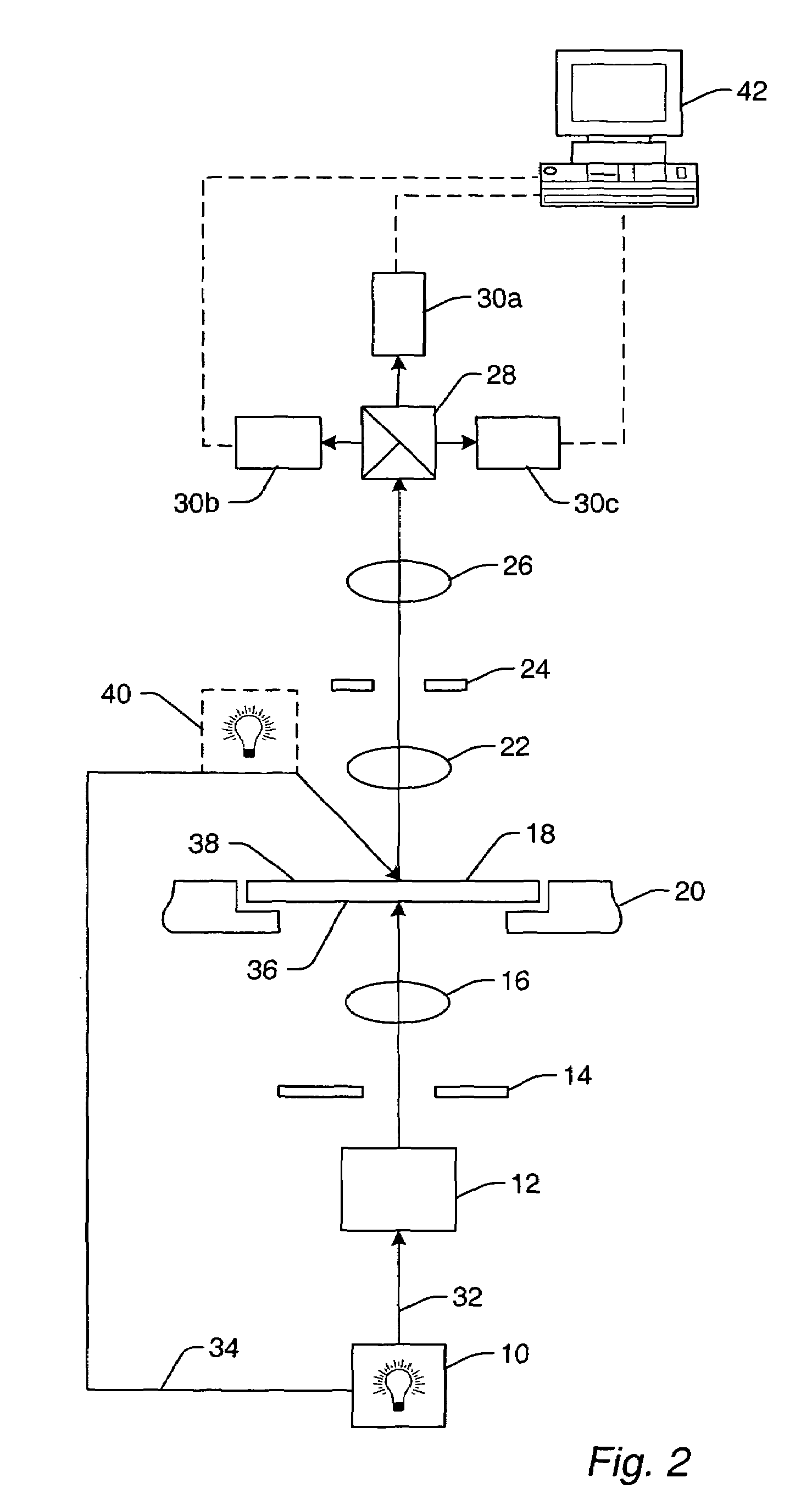
Apparatus and methods for inspecting reticles
PatentActiveUS20180082415A1
Innovation
- A method and system for qualifying photolithographic reticles by acquiring images at different illumination and imaging configurations to recover the reticle near field, which is then analyzed to determine potential wafer pattern defects and stability, using a lithography model to simulate wafer images and compare them under various process conditions.


Methods and systems for reticle inspection and defect review using aerial imaging
PatentInactiveUS7379175B1
Innovation
- A method and system for inspecting reticles using aerial imaging, where a set of exposure conditions forms an aerial image of the reticle, and defects are detected by comparing this image to a reference image stored in a database, excluding optical proximity correction features, allowing for the identification of defects that would be printed onto a specimen.

Semiconductor Manufacturing Quality Standards Impact
The implementation of advanced reticle inspection protocols fundamentally transforms semiconductor manufacturing quality standards by establishing more stringent accuracy requirements and comprehensive validation frameworks. These enhanced protocols necessitate the development of new quality metrics that extend beyond traditional defect detection to encompass dimensional accuracy, pattern fidelity, and systematic error characterization across the entire reticle surface.
Quality standards evolution reflects the industry's transition toward more sophisticated inspection methodologies that integrate multiple measurement techniques and real-time feedback mechanisms. The redesigned protocols mandate higher resolution inspection capabilities, requiring quality frameworks to accommodate sub-nanometer precision requirements and establish new tolerance bands for critical dimension uniformity. This shift compels manufacturers to adopt more rigorous statistical process control methods and implement advanced data analytics for quality assessment.
The impact on manufacturing quality standards extends to the establishment of new certification requirements for inspection equipment and personnel training protocols. Quality assurance frameworks must now incorporate machine learning-based anomaly detection algorithms and predictive maintenance schedules to ensure consistent inspection performance. These standards also mandate comprehensive documentation of inspection parameters, environmental conditions, and calibration procedures to maintain traceability and reproducibility.
Regulatory compliance frameworks undergo significant modifications to accommodate the enhanced inspection capabilities and data requirements. Quality standards now emphasize the integration of inspection data with manufacturing execution systems, enabling real-time quality monitoring and automated decision-making processes. This integration requires new data integrity protocols and cybersecurity measures to protect sensitive manufacturing information while maintaining quality transparency.
The economic implications of these quality standard changes include increased capital investment requirements for advanced inspection equipment and extended qualification timelines for new manufacturing processes. However, the enhanced quality standards ultimately reduce downstream manufacturing costs by minimizing defective wafer production and improving overall yield performance, creating a positive return on investment for semiconductor manufacturers adopting these advanced protocols.
Quality standards evolution reflects the industry's transition toward more sophisticated inspection methodologies that integrate multiple measurement techniques and real-time feedback mechanisms. The redesigned protocols mandate higher resolution inspection capabilities, requiring quality frameworks to accommodate sub-nanometer precision requirements and establish new tolerance bands for critical dimension uniformity. This shift compels manufacturers to adopt more rigorous statistical process control methods and implement advanced data analytics for quality assessment.
The impact on manufacturing quality standards extends to the establishment of new certification requirements for inspection equipment and personnel training protocols. Quality assurance frameworks must now incorporate machine learning-based anomaly detection algorithms and predictive maintenance schedules to ensure consistent inspection performance. These standards also mandate comprehensive documentation of inspection parameters, environmental conditions, and calibration procedures to maintain traceability and reproducibility.
Regulatory compliance frameworks undergo significant modifications to accommodate the enhanced inspection capabilities and data requirements. Quality standards now emphasize the integration of inspection data with manufacturing execution systems, enabling real-time quality monitoring and automated decision-making processes. This integration requires new data integrity protocols and cybersecurity measures to protect sensitive manufacturing information while maintaining quality transparency.
The economic implications of these quality standard changes include increased capital investment requirements for advanced inspection equipment and extended qualification timelines for new manufacturing processes. However, the enhanced quality standards ultimately reduce downstream manufacturing costs by minimizing defective wafer production and improving overall yield performance, creating a positive return on investment for semiconductor manufacturers adopting these advanced protocols.
Cost-Benefit Analysis of Advanced Inspection Protocols
The implementation of advanced reticle inspection protocols requires substantial capital investment, yet the economic justification becomes compelling when analyzing long-term operational benefits. Initial equipment costs for next-generation inspection systems typically range from $15-25 million per unit, with additional infrastructure modifications adding 20-30% to the base investment. However, these systems deliver measurable returns through enhanced defect detection capabilities that prevent costly downstream failures.
Operational cost analysis reveals significant efficiency gains through automated inspection workflows. Advanced protocols reduce manual inspection time by 60-70%, translating to labor cost savings of approximately $2-3 million annually for high-volume manufacturing facilities. The integration of AI-driven defect classification further minimizes false positive rates, reducing unnecessary reticle cleaning cycles and extending reticle lifespan by 25-40%.
Quality-related cost benefits demonstrate the most substantial economic impact. Traditional inspection methods miss critical defects that can cause yield losses exceeding $10-15 million per affected lot in advanced node production. Enhanced inspection protocols achieve defect detection rates above 95%, compared to 75-80% for conventional systems, directly preventing these catastrophic yield events.
Risk mitigation analysis shows reduced insurance premiums and customer penalty exposure. Manufacturing facilities implementing advanced protocols report 40-50% reduction in quality-related incidents, leading to improved customer satisfaction scores and contract renewal rates. The enhanced traceability and documentation capabilities also provide valuable intellectual property protection and regulatory compliance benefits.
Return on investment calculations indicate payback periods of 18-24 months for high-volume production environments. The combination of prevented yield losses, operational efficiency gains, and extended equipment lifecycles creates a compelling business case. Additionally, the competitive advantage gained through superior quality control capabilities enables premium pricing strategies and market share expansion opportunities.
Long-term strategic benefits include reduced total cost of ownership through predictive maintenance capabilities and optimized inspection scheduling. These advanced protocols enable data-driven decision making that further enhances operational efficiency and cost management across the entire manufacturing ecosystem.
Operational cost analysis reveals significant efficiency gains through automated inspection workflows. Advanced protocols reduce manual inspection time by 60-70%, translating to labor cost savings of approximately $2-3 million annually for high-volume manufacturing facilities. The integration of AI-driven defect classification further minimizes false positive rates, reducing unnecessary reticle cleaning cycles and extending reticle lifespan by 25-40%.
Quality-related cost benefits demonstrate the most substantial economic impact. Traditional inspection methods miss critical defects that can cause yield losses exceeding $10-15 million per affected lot in advanced node production. Enhanced inspection protocols achieve defect detection rates above 95%, compared to 75-80% for conventional systems, directly preventing these catastrophic yield events.
Risk mitigation analysis shows reduced insurance premiums and customer penalty exposure. Manufacturing facilities implementing advanced protocols report 40-50% reduction in quality-related incidents, leading to improved customer satisfaction scores and contract renewal rates. The enhanced traceability and documentation capabilities also provide valuable intellectual property protection and regulatory compliance benefits.
Return on investment calculations indicate payback periods of 18-24 months for high-volume production environments. The combination of prevented yield losses, operational efficiency gains, and extended equipment lifecycles creates a compelling business case. Additionally, the competitive advantage gained through superior quality control capabilities enables premium pricing strategies and market share expansion opportunities.
Long-term strategic benefits include reduced total cost of ownership through predictive maintenance capabilities and optimized inspection scheduling. These advanced protocols enable data-driven decision making that further enhances operational efficiency and cost management across the entire manufacturing ecosystem.
Unlock deeper insights with PatSnap Eureka Quick Research — get a full tech report to explore trends and direct your research. Try now!
Generate Your Research Report Instantly with AI Agent
Supercharge your innovation with PatSnap Eureka AI Agent Platform!