

Optimizing Inspection Algorithms for Faster Analysis in Advanced Reticle Tools
MAY 20, 20269 MIN READ
Generate Your Research Report Instantly with AI Agent
PatSnap Eureka helps you evaluate technical feasibility & market potential.
Reticle Inspection Technology Background and Objectives
Reticle inspection technology has evolved as a critical component in semiconductor manufacturing, serving as the foundation for ensuring pattern fidelity and defect-free photomasks used in lithography processes. The technology emerged in the 1980s alongside the advancement of integrated circuit manufacturing, when feature sizes began shrinking and the tolerance for defects became increasingly stringent. Early inspection systems relied on optical microscopy and basic pattern matching algorithms, but the exponential growth in chip complexity and the transition to advanced nodes below 28nm have necessitated revolutionary improvements in both hardware capabilities and algorithmic sophistication.
The fundamental objective of modern reticle inspection systems centers on achieving comprehensive defect detection while maintaining economically viable throughput rates. Traditional inspection approaches face significant challenges as they must balance three competing requirements: detection sensitivity for sub-wavelength defects, inspection speed to meet production demands, and false alarm rates that do not overwhelm review capacity. Current advanced reticle tools employ multi-beam electron microscopy, high-resolution optical systems, and sophisticated image processing algorithms to detect critical defects including pattern breaks, bridging, line edge roughness variations, and contamination particles.
The primary technical goal driving current research focuses on optimizing inspection algorithms to reduce analysis time without compromising defect detection capability. This optimization challenge encompasses multiple dimensions including algorithm efficiency, parallel processing implementation, machine learning integration, and adaptive inspection strategies. Advanced algorithms must process terabytes of high-resolution image data while identifying defects that may be only a few nanometers in size, requiring sophisticated signal processing techniques and pattern recognition methodologies.
Contemporary inspection systems target sub-10nm defect detection capabilities with throughput rates exceeding one reticle per hour for the most critical layers. The integration of artificial intelligence and deep learning approaches represents a paradigm shift from traditional rule-based algorithms toward adaptive systems that can learn from historical defect patterns and optimize inspection parameters in real-time. These technological objectives align with the semiconductor industry's roadmap requirements for supporting next-generation lithography processes including extreme ultraviolet lithography and advanced packaging technologies.
The fundamental objective of modern reticle inspection systems centers on achieving comprehensive defect detection while maintaining economically viable throughput rates. Traditional inspection approaches face significant challenges as they must balance three competing requirements: detection sensitivity for sub-wavelength defects, inspection speed to meet production demands, and false alarm rates that do not overwhelm review capacity. Current advanced reticle tools employ multi-beam electron microscopy, high-resolution optical systems, and sophisticated image processing algorithms to detect critical defects including pattern breaks, bridging, line edge roughness variations, and contamination particles.
The primary technical goal driving current research focuses on optimizing inspection algorithms to reduce analysis time without compromising defect detection capability. This optimization challenge encompasses multiple dimensions including algorithm efficiency, parallel processing implementation, machine learning integration, and adaptive inspection strategies. Advanced algorithms must process terabytes of high-resolution image data while identifying defects that may be only a few nanometers in size, requiring sophisticated signal processing techniques and pattern recognition methodologies.
Contemporary inspection systems target sub-10nm defect detection capabilities with throughput rates exceeding one reticle per hour for the most critical layers. The integration of artificial intelligence and deep learning approaches represents a paradigm shift from traditional rule-based algorithms toward adaptive systems that can learn from historical defect patterns and optimize inspection parameters in real-time. These technological objectives align with the semiconductor industry's roadmap requirements for supporting next-generation lithography processes including extreme ultraviolet lithography and advanced packaging technologies.
Market Demand for Advanced Reticle Inspection Solutions
The semiconductor industry's relentless pursuit of smaller node technologies has created unprecedented demand for advanced reticle inspection solutions. As chip manufacturers transition to extreme ultraviolet lithography and sub-3nm processes, the tolerance for defects on photomasks has decreased exponentially, driving the need for more sophisticated inspection capabilities that can detect increasingly minute anomalies while maintaining production throughput.
Current market dynamics reveal a significant bottleneck in reticle inspection workflows, where traditional algorithms struggle to balance detection sensitivity with analysis speed. Leading semiconductor fabs report that inspection cycle times have become a critical constraint in mask production schedules, particularly for advanced logic and memory devices where mask complexity continues to escalate. The industry faces mounting pressure to reduce time-to-market while ensuring zero-defect manufacturing standards.
The emergence of artificial intelligence and machine learning technologies has opened new avenues for inspection algorithm optimization. Market participants are actively seeking solutions that leverage deep learning architectures to accelerate pattern recognition and defect classification processes. This technological shift represents a fundamental departure from conventional rule-based inspection methodologies, promising substantial improvements in both speed and accuracy metrics.
Foundry operators and integrated device manufacturers have identified inspection throughput as a key differentiator in competitive positioning. The ability to process complex reticle patterns rapidly while maintaining detection reliability directly impacts manufacturing capacity and cost structures. Market research indicates that inspection speed improvements of even modest percentages can translate to significant operational advantages and revenue opportunities.
The growing complexity of multi-patterning techniques and advanced packaging technologies further amplifies the demand for optimized inspection algorithms. These emerging applications require inspection systems capable of handling diverse pattern geometries and material compositions simultaneously, necessitating algorithmic approaches that can adapt dynamically to varying inspection requirements without compromising performance standards.
Supply chain considerations also drive market demand, as semiconductor manufacturers seek to reduce dependency on extended inspection cycles that can create production bottlenecks. The industry's shift toward more distributed manufacturing models requires inspection solutions that can deliver consistent performance across multiple facilities while accommodating varying operational parameters and quality requirements.
Current market dynamics reveal a significant bottleneck in reticle inspection workflows, where traditional algorithms struggle to balance detection sensitivity with analysis speed. Leading semiconductor fabs report that inspection cycle times have become a critical constraint in mask production schedules, particularly for advanced logic and memory devices where mask complexity continues to escalate. The industry faces mounting pressure to reduce time-to-market while ensuring zero-defect manufacturing standards.
The emergence of artificial intelligence and machine learning technologies has opened new avenues for inspection algorithm optimization. Market participants are actively seeking solutions that leverage deep learning architectures to accelerate pattern recognition and defect classification processes. This technological shift represents a fundamental departure from conventional rule-based inspection methodologies, promising substantial improvements in both speed and accuracy metrics.
Foundry operators and integrated device manufacturers have identified inspection throughput as a key differentiator in competitive positioning. The ability to process complex reticle patterns rapidly while maintaining detection reliability directly impacts manufacturing capacity and cost structures. Market research indicates that inspection speed improvements of even modest percentages can translate to significant operational advantages and revenue opportunities.
The growing complexity of multi-patterning techniques and advanced packaging technologies further amplifies the demand for optimized inspection algorithms. These emerging applications require inspection systems capable of handling diverse pattern geometries and material compositions simultaneously, necessitating algorithmic approaches that can adapt dynamically to varying inspection requirements without compromising performance standards.
Supply chain considerations also drive market demand, as semiconductor manufacturers seek to reduce dependency on extended inspection cycles that can create production bottlenecks. The industry's shift toward more distributed manufacturing models requires inspection solutions that can deliver consistent performance across multiple facilities while accommodating varying operational parameters and quality requirements.
Current State and Challenges of Inspection Algorithms
Advanced reticle inspection algorithms currently operate within a complex technological landscape where precision requirements continue to escalate alongside manufacturing node shrinkage. Contemporary inspection systems predominantly rely on die-to-die and die-to-database comparison methodologies, utilizing high-resolution optical and electron beam technologies to detect defects at nanometer scales. These algorithms must process massive datasets while maintaining detection sensitivity for critical dimension variations, pattern placement errors, and contamination particles that could impact semiconductor yield.
The computational architecture of existing inspection algorithms faces significant performance bottlenecks due to the exponential growth in data volume generated by advanced imaging systems. Current systems typically process inspection data through sequential analysis pipelines, where image acquisition, preprocessing, feature extraction, and defect classification occur in largely linear workflows. This approach results in substantial processing delays, particularly when handling the complex geometries and dense patterns characteristic of sub-7nm technology nodes.
Algorithm accuracy presents another fundamental challenge, as false positive rates directly impact manufacturing throughput and cost efficiency. Existing detection algorithms struggle to differentiate between actual defects and acceptable process variations, leading to unnecessary wafer scrapping or missed critical defects. The sensitivity-specificity trade-off becomes increasingly problematic as pattern complexity increases, requiring more sophisticated classification models that inherently demand greater computational resources.
Real-time processing constraints impose severe limitations on current inspection capabilities. Advanced reticle tools generate terabytes of inspection data per session, yet manufacturing timelines demand rapid turnaround for production decisions. Conventional algorithms often require offline processing or significant time delays, creating bottlenecks in the manufacturing workflow that impact overall fab productivity and cycle times.
Machine learning integration represents both an opportunity and a challenge within current inspection frameworks. While deep learning approaches show promise for improved defect classification accuracy, their implementation requires extensive training datasets and computational infrastructure that many existing systems cannot accommodate. The black-box nature of neural network models also creates challenges for process control and regulatory compliance in semiconductor manufacturing environments.
Scalability issues emerge as inspection requirements expand across multiple technology nodes and product types. Current algorithms often require extensive recalibration and parameter adjustment when transitioning between different reticle types or manufacturing processes, limiting their flexibility and increasing operational complexity. The lack of standardized interfaces and data formats further complicates algorithm deployment across diverse inspection platforms.
The computational architecture of existing inspection algorithms faces significant performance bottlenecks due to the exponential growth in data volume generated by advanced imaging systems. Current systems typically process inspection data through sequential analysis pipelines, where image acquisition, preprocessing, feature extraction, and defect classification occur in largely linear workflows. This approach results in substantial processing delays, particularly when handling the complex geometries and dense patterns characteristic of sub-7nm technology nodes.
Algorithm accuracy presents another fundamental challenge, as false positive rates directly impact manufacturing throughput and cost efficiency. Existing detection algorithms struggle to differentiate between actual defects and acceptable process variations, leading to unnecessary wafer scrapping or missed critical defects. The sensitivity-specificity trade-off becomes increasingly problematic as pattern complexity increases, requiring more sophisticated classification models that inherently demand greater computational resources.
Real-time processing constraints impose severe limitations on current inspection capabilities. Advanced reticle tools generate terabytes of inspection data per session, yet manufacturing timelines demand rapid turnaround for production decisions. Conventional algorithms often require offline processing or significant time delays, creating bottlenecks in the manufacturing workflow that impact overall fab productivity and cycle times.
Machine learning integration represents both an opportunity and a challenge within current inspection frameworks. While deep learning approaches show promise for improved defect classification accuracy, their implementation requires extensive training datasets and computational infrastructure that many existing systems cannot accommodate. The black-box nature of neural network models also creates challenges for process control and regulatory compliance in semiconductor manufacturing environments.
Scalability issues emerge as inspection requirements expand across multiple technology nodes and product types. Current algorithms often require extensive recalibration and parameter adjustment when transitioning between different reticle types or manufacturing processes, limiting their flexibility and increasing operational complexity. The lack of standardized interfaces and data formats further complicates algorithm deployment across diverse inspection platforms.
Current Algorithm Optimization Solutions for Reticles
01 Real-time inspection algorithms optimization
Advanced algorithms designed to optimize inspection processes in real-time environments, focusing on reducing computational overhead while maintaining accuracy. These methods employ streamlined processing techniques and efficient data structures to accelerate analysis workflows. The algorithms incorporate adaptive sampling and intelligent filtering mechanisms to minimize processing time without compromising detection quality.- Real-time inspection algorithm optimization: Advanced algorithms designed to optimize inspection processes in real-time environments, focusing on reducing computational overhead while maintaining accuracy. These methods employ streamlined data processing techniques and efficient memory management to achieve faster analysis speeds without compromising detection quality.
- Parallel processing and multi-threading techniques: Implementation of parallel computing architectures and multi-threading approaches to accelerate inspection algorithm performance. These techniques distribute computational workload across multiple processors or cores, enabling simultaneous processing of different data segments to significantly reduce overall analysis time.
- Machine learning acceleration for inspection systems: Integration of optimized machine learning models and neural network architectures specifically designed for high-speed inspection applications. These systems utilize hardware acceleration, model compression, and inference optimization techniques to achieve rapid pattern recognition and defect detection capabilities.
- Hardware-software co-optimization strategies: Comprehensive approaches that combine specialized hardware configurations with tailored software implementations to maximize inspection algorithm efficiency. These strategies involve custom processor designs, dedicated memory architectures, and algorithm-specific optimizations to achieve optimal speed-accuracy trade-offs.
- Adaptive sampling and data reduction methods: Intelligent sampling techniques and data preprocessing methods that reduce the computational burden on inspection algorithms by selectively processing relevant information. These approaches use statistical analysis, feature extraction, and adaptive filtering to minimize data volume while preserving critical inspection accuracy.
02 Parallel processing and multi-threading techniques
Implementation of parallel computing architectures and multi-threading approaches to enhance inspection algorithm performance. These techniques distribute computational loads across multiple processors or cores, significantly reducing analysis time for complex inspection tasks. The methods include load balancing strategies and synchronized processing frameworks that maximize hardware utilization efficiency.Expand Specific Solutions03 Machine learning acceleration for inspection analysis
Integration of machine learning models and artificial intelligence techniques to accelerate inspection algorithms through predictive analysis and pattern recognition. These approaches utilize trained neural networks and deep learning frameworks to rapidly identify defects and anomalies. The systems employ optimized inference engines and model compression techniques to achieve faster processing speeds while maintaining high accuracy rates.Expand Specific Solutions04 Hardware-accelerated inspection processing
Utilization of specialized hardware components such as graphics processing units, field-programmable gate arrays, and dedicated signal processors to accelerate inspection algorithms. These implementations leverage hardware-specific optimizations and custom instruction sets to achieve superior performance compared to traditional software-only solutions. The approaches include pipeline architectures and dedicated computational units designed specifically for inspection tasks.Expand Specific Solutions05 Adaptive algorithm optimization and caching strategies
Development of self-optimizing inspection algorithms that adapt their processing strategies based on input characteristics and system performance metrics. These methods incorporate intelligent caching mechanisms, predictive prefetching, and dynamic algorithm selection to minimize computational requirements. The systems feature adaptive threshold adjustment and context-aware processing that automatically tune parameters for optimal speed-accuracy trade-offs.Expand Specific Solutions
Key Players in Reticle Inspection Equipment Industry
The advanced reticle inspection algorithm optimization market represents a mature, high-value segment within semiconductor manufacturing, driven by increasing demand for precision lithography in sub-7nm processes. The industry is in a consolidation phase with market size exceeding $2 billion annually, dominated by established equipment manufacturers. Technology maturity varies significantly across players: Applied Materials and Applied Materials Israel Ltd. lead with cutting-edge AI-enhanced inspection algorithms, while Samsung Electronics and SCREEN Holdings demonstrate strong integration capabilities. Evident Corp. brings advanced microscopy expertise, and Shanghai Huali Microelectronics represents emerging foundry requirements. The competitive landscape shows clear technological stratification, with tier-one suppliers like Applied Materials commanding premium positioning through superior algorithm performance and processing speed, while regional players focus on cost-effective solutions for specific market segments.
SCREEN Holdings Co., Ltd.
Technical Solution: SCREEN Holdings has developed inspection algorithms specifically designed for photomask and reticle quality control, incorporating advanced image processing techniques and statistical pattern recognition. Their systems utilize multi-wavelength inspection technology combined with machine learning algorithms to detect defects as small as 15nm while processing up to 80 reticles per day. The algorithms feature automated defect classification with over 95% accuracy and real-time process feedback mechanisms that enable continuous optimization of inspection parameters for different reticle types and manufacturing requirements.
Strengths: Specialized photomask expertise, high-accuracy defect classification systems. Weaknesses: Smaller market presence compared to major competitors, limited global service network.
Applied Materials, Inc.
Technical Solution: Applied Materials has developed advanced reticle inspection algorithms utilizing machine learning and AI-powered defect detection systems. Their inspection tools employ multi-beam electron microscopy combined with high-speed parallel processing architectures to achieve sub-10nm defect detection capabilities. The company's proprietary algorithms incorporate adaptive thresholding techniques and pattern recognition systems that can process inspection data at rates exceeding 100 wafers per hour while maintaining detection sensitivity below 20nm for critical defects.
Strengths: Industry-leading detection sensitivity and throughput rates, comprehensive defect classification capabilities. Weaknesses: High capital investment requirements and complex system integration needs.
Core Algorithm Innovations for Faster Reticle Analysis
Optimization of the recipe of an examination tool
PatentPendingKR1020240109592A
Innovation
- An automated system determines optimal dimensions for acquiring slices of semiconductor specimens, minimizing slice overlap and maximizing parallel computing power to improve throughput by fusing multiple dies into regions, using a processor and memory circuit to create an optimized inspection recipe.


Methods and systems for reticle inspection and defect review using aerial imaging
PatentInactiveUS7379175B1
Innovation
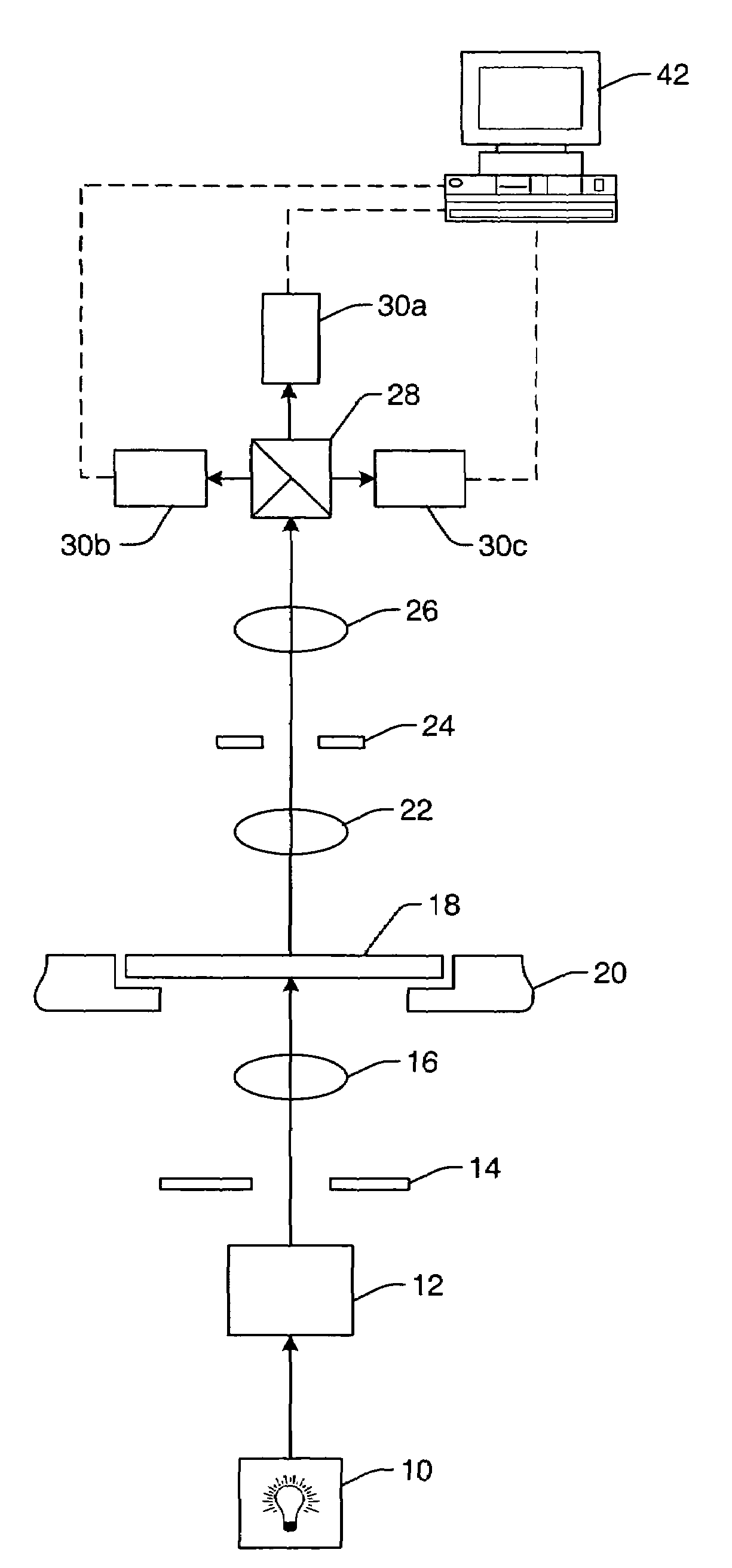
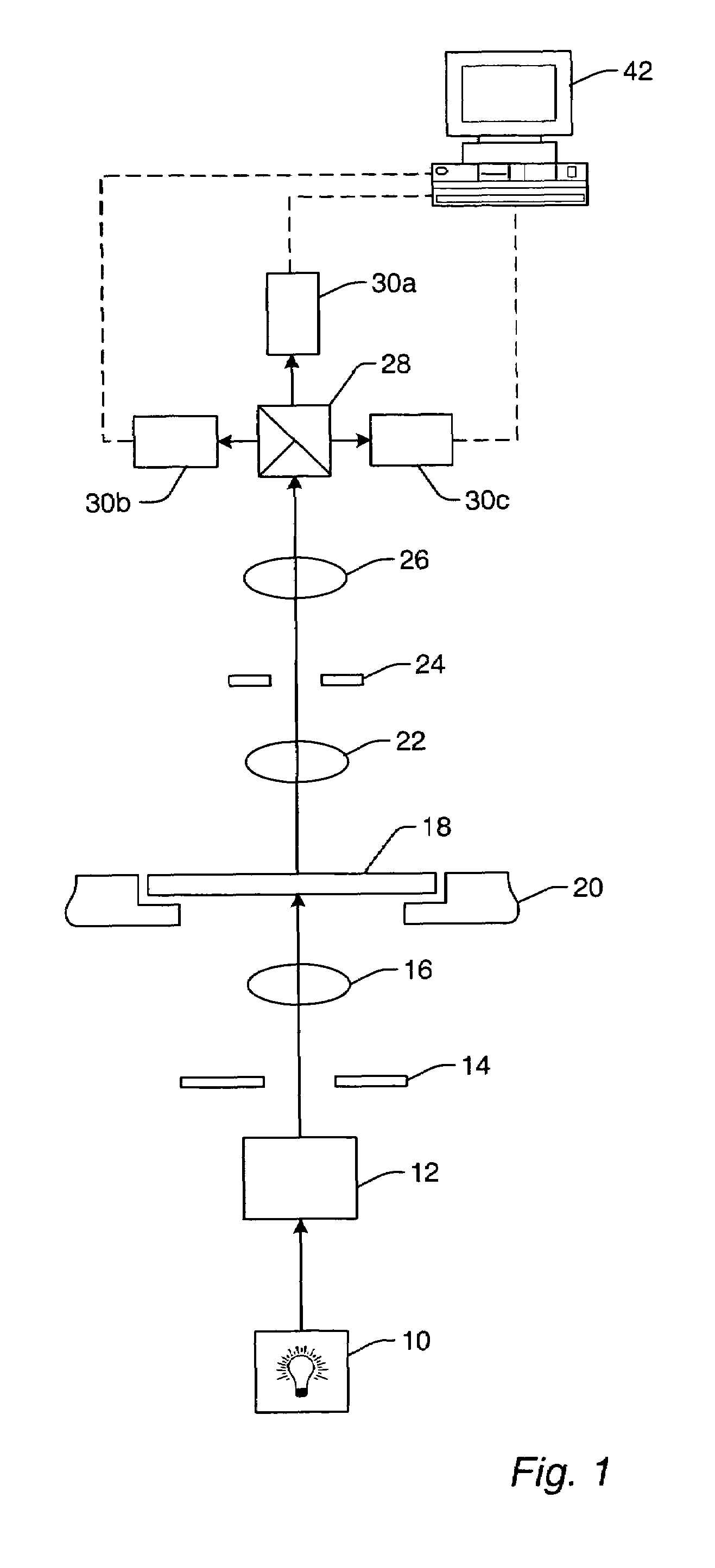
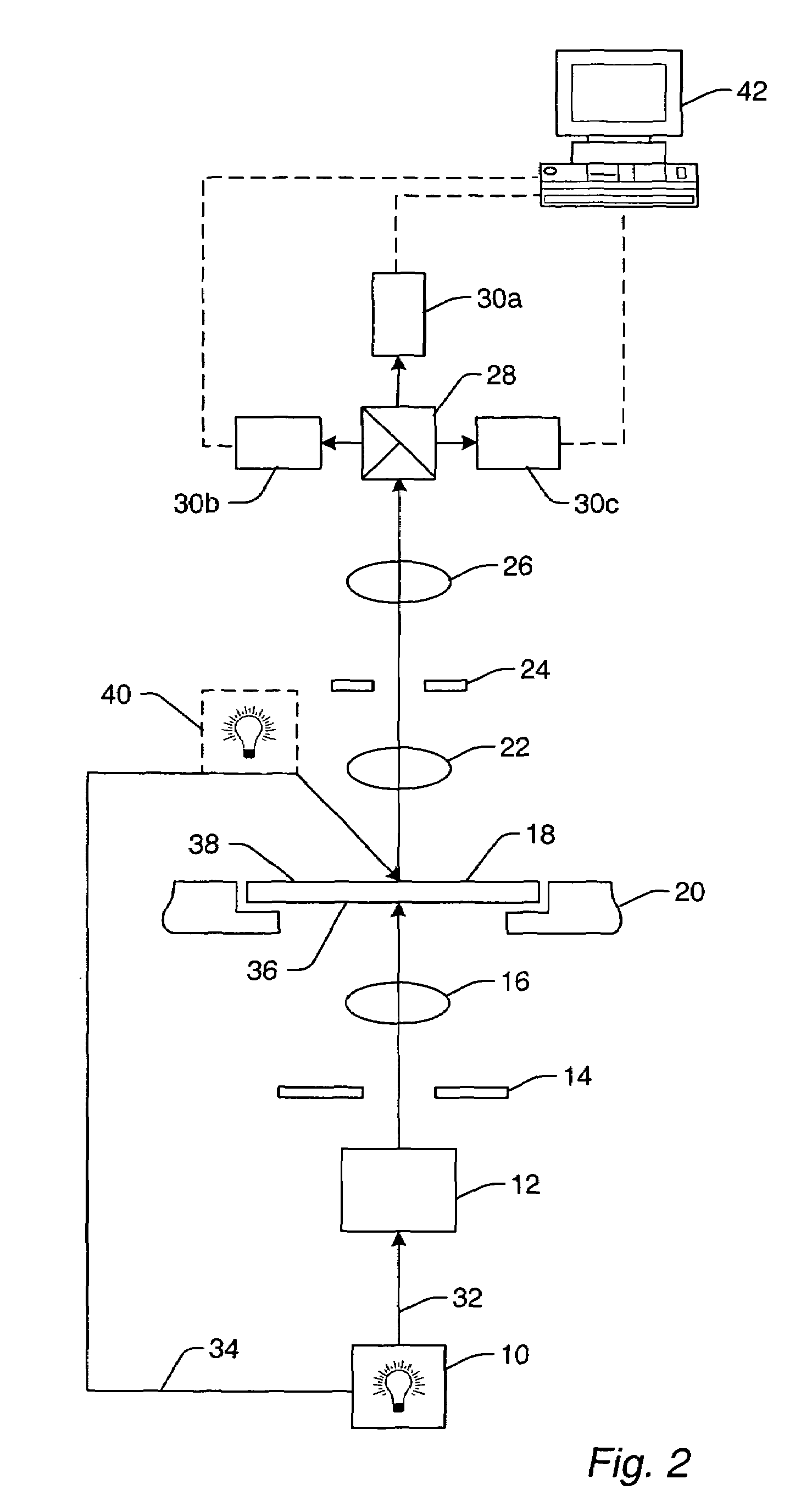
- A method and system for inspecting reticles using aerial imaging, where a set of exposure conditions forms an aerial image of the reticle, and defects are detected by comparing this image to a reference image stored in a database, excluding optical proximity correction features, allowing for the identification of defects that would be printed onto a specimen.

Semiconductor Industry Standards and Compliance
The semiconductor industry operates under stringent regulatory frameworks that directly impact the development and deployment of advanced reticle inspection algorithms. International standards organizations such as SEMI, ISO, and IEC establish comprehensive guidelines for semiconductor manufacturing equipment, including specifications for measurement accuracy, repeatability, and traceability requirements that inspection algorithms must satisfy.
SEMI standards, particularly SEMI E10 for specification and guidelines for equipment suppliers and SEMI E30 for generic model for communications and control of manufacturing equipment, provide foundational requirements for inspection tool performance. These standards mandate specific algorithmic validation protocols, including statistical process control metrics and defect detection sensitivity thresholds that optimization efforts must maintain or exceed.
Compliance with ISO 9001 quality management systems requires documented validation of algorithm modifications, establishing clear traceability between optimization changes and performance outcomes. The semiconductor industry's adoption of ISO/TS 16949 automotive quality standards further emphasizes the need for robust algorithm validation processes, particularly for reticle tools serving automotive semiconductor applications.
Regional regulatory variations significantly influence algorithm optimization strategies. European REACH regulations impact material composition requirements for inspection systems, while U.S. export control regulations under EAR and ITAR affect the development and deployment of advanced inspection algorithms in global manufacturing environments. These compliance requirements often necessitate algorithm modifications to ensure data security and technology transfer restrictions are maintained.
Industry-specific standards such as JEDEC publications provide detailed specifications for semiconductor device reliability and testing methodologies. Algorithm optimization must align with these standards to ensure inspection results meet industry-accepted criteria for defect classification and measurement precision. The International Roadmap for Devices and Systems further establishes performance benchmarks that drive algorithm development priorities.
Emerging standards for artificial intelligence and machine learning applications in semiconductor manufacturing are beginning to influence inspection algorithm development. These evolving frameworks address algorithm transparency, bias mitigation, and performance validation requirements that optimization efforts must increasingly consider to maintain industry compliance and customer acceptance.
SEMI standards, particularly SEMI E10 for specification and guidelines for equipment suppliers and SEMI E30 for generic model for communications and control of manufacturing equipment, provide foundational requirements for inspection tool performance. These standards mandate specific algorithmic validation protocols, including statistical process control metrics and defect detection sensitivity thresholds that optimization efforts must maintain or exceed.
Compliance with ISO 9001 quality management systems requires documented validation of algorithm modifications, establishing clear traceability between optimization changes and performance outcomes. The semiconductor industry's adoption of ISO/TS 16949 automotive quality standards further emphasizes the need for robust algorithm validation processes, particularly for reticle tools serving automotive semiconductor applications.
Regional regulatory variations significantly influence algorithm optimization strategies. European REACH regulations impact material composition requirements for inspection systems, while U.S. export control regulations under EAR and ITAR affect the development and deployment of advanced inspection algorithms in global manufacturing environments. These compliance requirements often necessitate algorithm modifications to ensure data security and technology transfer restrictions are maintained.
Industry-specific standards such as JEDEC publications provide detailed specifications for semiconductor device reliability and testing methodologies. Algorithm optimization must align with these standards to ensure inspection results meet industry-accepted criteria for defect classification and measurement precision. The International Roadmap for Devices and Systems further establishes performance benchmarks that drive algorithm development priorities.
Emerging standards for artificial intelligence and machine learning applications in semiconductor manufacturing are beginning to influence inspection algorithm development. These evolving frameworks address algorithm transparency, bias mitigation, and performance validation requirements that optimization efforts must increasingly consider to maintain industry compliance and customer acceptance.
Cost-Performance Trade-offs in Algorithm Optimization
The optimization of inspection algorithms for advanced reticle tools presents a complex landscape of cost-performance trade-offs that significantly impact both operational efficiency and economic viability. These trade-offs manifest across multiple dimensions, requiring careful consideration of computational resources, processing speed, detection accuracy, and implementation costs.
Computational complexity represents the primary driver of cost-performance dynamics in algorithm optimization. High-performance algorithms typically demand substantial processing power, memory bandwidth, and specialized hardware accelerators, leading to increased capital expenditure and operational costs. Advanced machine learning models, while offering superior defect detection capabilities, require extensive GPU clusters or dedicated AI chips that can cost millions of dollars for enterprise-scale deployments.
Processing speed optimization often involves algorithmic simplifications that may compromise detection sensitivity or introduce false positive rates. Faster algorithms frequently employ approximation techniques, reduced sampling rates, or simplified feature extraction methods to achieve real-time performance targets. This creates a fundamental tension between throughput requirements and inspection quality, where manufacturers must balance production line efficiency against potential yield losses from missed defects.
Memory utilization presents another critical trade-off dimension. High-resolution reticle inspection generates massive datasets requiring sophisticated buffering and caching strategies. Algorithms optimized for minimal memory footprint may sacrifice processing parallelism or require multiple data passes, ultimately impacting overall system performance. Conversely, memory-intensive approaches can achieve superior speed but demand expensive high-bandwidth memory systems.
Implementation complexity directly correlates with development and maintenance costs. Sophisticated optimization techniques such as adaptive thresholding, multi-scale analysis, or ensemble methods require specialized expertise and extended development cycles. Organizations must weigh the long-term performance benefits against increased software development costs, training requirements, and ongoing maintenance overhead.
The economic impact extends beyond direct implementation costs to include opportunity costs associated with algorithm selection. Conservative approaches may result in over-inspection, reducing throughput and increasing per-unit inspection costs. Aggressive optimization strategies risk under-detection, potentially leading to costly downstream failures and customer quality issues that far exceed initial savings from faster processing.
Computational complexity represents the primary driver of cost-performance dynamics in algorithm optimization. High-performance algorithms typically demand substantial processing power, memory bandwidth, and specialized hardware accelerators, leading to increased capital expenditure and operational costs. Advanced machine learning models, while offering superior defect detection capabilities, require extensive GPU clusters or dedicated AI chips that can cost millions of dollars for enterprise-scale deployments.
Processing speed optimization often involves algorithmic simplifications that may compromise detection sensitivity or introduce false positive rates. Faster algorithms frequently employ approximation techniques, reduced sampling rates, or simplified feature extraction methods to achieve real-time performance targets. This creates a fundamental tension between throughput requirements and inspection quality, where manufacturers must balance production line efficiency against potential yield losses from missed defects.
Memory utilization presents another critical trade-off dimension. High-resolution reticle inspection generates massive datasets requiring sophisticated buffering and caching strategies. Algorithms optimized for minimal memory footprint may sacrifice processing parallelism or require multiple data passes, ultimately impacting overall system performance. Conversely, memory-intensive approaches can achieve superior speed but demand expensive high-bandwidth memory systems.
Implementation complexity directly correlates with development and maintenance costs. Sophisticated optimization techniques such as adaptive thresholding, multi-scale analysis, or ensemble methods require specialized expertise and extended development cycles. Organizations must weigh the long-term performance benefits against increased software development costs, training requirements, and ongoing maintenance overhead.
The economic impact extends beyond direct implementation costs to include opportunity costs associated with algorithm selection. Conservative approaches may result in over-inspection, reducing throughput and increasing per-unit inspection costs. Aggressive optimization strategies risk under-detection, potentially leading to costly downstream failures and customer quality issues that far exceed initial savings from faster processing.
Unlock deeper insights with PatSnap Eureka Quick Research — get a full tech report to explore trends and direct your research. Try now!
Generate Your Research Report Instantly with AI Agent
Supercharge your innovation with PatSnap Eureka AI Agent Platform!