

Advanced Reticle Inspection: Which Method Provides Sub-Pixel Quality Detection?
MAY 20, 20269 MIN READ
Generate Your Research Report Instantly with AI Agent
PatSnap Eureka helps you evaluate technical feasibility & market potential.
Advanced Reticle Inspection Technology Background and Objectives
Advanced reticle inspection technology has emerged as a critical component in semiconductor manufacturing, driven by the relentless pursuit of smaller feature sizes and higher device densities. As the semiconductor industry continues to push the boundaries of Moore's Law, the demand for increasingly sophisticated photomasks has intensified, necessitating inspection capabilities that can detect defects at sub-pixel resolution levels.
The evolution of reticle inspection began in the 1980s with basic optical inspection systems capable of detecting relatively large defects. However, as technology nodes progressed from micron-scale to nanometer-scale dimensions, traditional inspection methods proved inadequate. The transition from 193nm lithography to extreme ultraviolet (EUV) lithography has further complicated the inspection landscape, requiring detection capabilities that can identify defects smaller than the wavelength of light used in the lithographic process.
Current market drivers for advanced reticle inspection stem from the exponential increase in mask complexity and the corresponding rise in manufacturing costs. Modern photomasks can cost upwards of several million dollars, making defect detection and prevention economically imperative. The industry's shift toward 7nm, 5nm, and 3nm process nodes has created unprecedented demands for inspection accuracy, with defect detection requirements now approaching atomic-scale precision.
The primary technical objective of contemporary reticle inspection systems centers on achieving sub-pixel quality detection capabilities. This involves developing methodologies that can identify and characterize defects significantly smaller than the pixel size of the inspection system's detector array. Sub-pixel detection is essential for ensuring that minute defects, which could potentially cause catastrophic failures in semiconductor devices, are identified before the costly lithographic process begins.
Key technological goals include enhancing signal-to-noise ratios in detection systems, improving algorithmic approaches for defect classification, and developing hybrid inspection methodologies that combine multiple detection techniques. The integration of artificial intelligence and machine learning algorithms has become increasingly important in achieving these objectives, enabling more sophisticated pattern recognition and defect classification capabilities.
The ultimate aim is to establish inspection systems capable of detecting defects with dimensions as small as 10-20% of the critical dimension being manufactured, while maintaining high throughput rates necessary for commercial viability. This requires balancing sensitivity, specificity, and speed in a technologically and economically feasible solution.
The evolution of reticle inspection began in the 1980s with basic optical inspection systems capable of detecting relatively large defects. However, as technology nodes progressed from micron-scale to nanometer-scale dimensions, traditional inspection methods proved inadequate. The transition from 193nm lithography to extreme ultraviolet (EUV) lithography has further complicated the inspection landscape, requiring detection capabilities that can identify defects smaller than the wavelength of light used in the lithographic process.
Current market drivers for advanced reticle inspection stem from the exponential increase in mask complexity and the corresponding rise in manufacturing costs. Modern photomasks can cost upwards of several million dollars, making defect detection and prevention economically imperative. The industry's shift toward 7nm, 5nm, and 3nm process nodes has created unprecedented demands for inspection accuracy, with defect detection requirements now approaching atomic-scale precision.
The primary technical objective of contemporary reticle inspection systems centers on achieving sub-pixel quality detection capabilities. This involves developing methodologies that can identify and characterize defects significantly smaller than the pixel size of the inspection system's detector array. Sub-pixel detection is essential for ensuring that minute defects, which could potentially cause catastrophic failures in semiconductor devices, are identified before the costly lithographic process begins.
Key technological goals include enhancing signal-to-noise ratios in detection systems, improving algorithmic approaches for defect classification, and developing hybrid inspection methodologies that combine multiple detection techniques. The integration of artificial intelligence and machine learning algorithms has become increasingly important in achieving these objectives, enabling more sophisticated pattern recognition and defect classification capabilities.
The ultimate aim is to establish inspection systems capable of detecting defects with dimensions as small as 10-20% of the critical dimension being manufactured, while maintaining high throughput rates necessary for commercial viability. This requires balancing sensitivity, specificity, and speed in a technologically and economically feasible solution.
Market Demand for Sub-Pixel Reticle Defect Detection
The semiconductor industry's relentless pursuit of smaller node technologies has created an unprecedented demand for sub-pixel reticle defect detection capabilities. As manufacturing processes advance toward 3nm and beyond, the critical dimensions of circuit patterns continue to shrink, making traditional inspection methods insufficient for detecting defects that could compromise yield and device performance. The industry requires inspection systems capable of identifying defects smaller than the optical resolution limit, driving significant market demand for advanced sub-pixel detection technologies.
Market drivers stem primarily from the economic impact of undetected reticle defects. A single defective reticle can potentially affect thousands of wafers, resulting in substantial financial losses for semiconductor manufacturers. Leading foundries and memory manufacturers are increasingly investing in next-generation inspection equipment to maintain competitive advantages and ensure product quality. The transition to extreme ultraviolet lithography has further intensified this demand, as EUV reticles require even more stringent defect control standards.
The automotive semiconductor sector represents another significant demand driver, where reliability requirements exceed traditional consumer electronics standards. Advanced driver assistance systems and autonomous vehicle components necessitate zero-defect manufacturing approaches, pushing automotive chip suppliers to adopt more sophisticated reticle inspection methodologies. This sector's growth trajectory continues to expand the addressable market for sub-pixel detection solutions.
Memory manufacturers face particular challenges with sub-pixel defect detection due to their high-volume production requirements and tight profit margins. The need to balance inspection thoroughness with manufacturing throughput has created demand for inspection systems that can achieve sub-pixel sensitivity while maintaining acceptable cycle times. This has led to increased adoption of hybrid inspection approaches combining multiple detection methodologies.
The market landscape shows strong regional concentration in Asia-Pacific, where major semiconductor manufacturing facilities are located. Taiwan, South Korea, and China represent the largest demand centers, with significant investments in advanced inspection infrastructure. However, equipment suppliers remain predominantly based in the United States, Europe, and Japan, creating a global supply-demand dynamic that influences market pricing and technology transfer considerations.
Emerging applications in artificial intelligence chips, high-performance computing processors, and advanced packaging technologies continue to expand market opportunities. These applications often require custom reticle designs with unique pattern geometries, creating specialized inspection challenges that drive demand for more flexible and sensitive detection systems capable of sub-pixel performance across diverse pattern types.
Market drivers stem primarily from the economic impact of undetected reticle defects. A single defective reticle can potentially affect thousands of wafers, resulting in substantial financial losses for semiconductor manufacturers. Leading foundries and memory manufacturers are increasingly investing in next-generation inspection equipment to maintain competitive advantages and ensure product quality. The transition to extreme ultraviolet lithography has further intensified this demand, as EUV reticles require even more stringent defect control standards.
The automotive semiconductor sector represents another significant demand driver, where reliability requirements exceed traditional consumer electronics standards. Advanced driver assistance systems and autonomous vehicle components necessitate zero-defect manufacturing approaches, pushing automotive chip suppliers to adopt more sophisticated reticle inspection methodologies. This sector's growth trajectory continues to expand the addressable market for sub-pixel detection solutions.
Memory manufacturers face particular challenges with sub-pixel defect detection due to their high-volume production requirements and tight profit margins. The need to balance inspection thoroughness with manufacturing throughput has created demand for inspection systems that can achieve sub-pixel sensitivity while maintaining acceptable cycle times. This has led to increased adoption of hybrid inspection approaches combining multiple detection methodologies.
The market landscape shows strong regional concentration in Asia-Pacific, where major semiconductor manufacturing facilities are located. Taiwan, South Korea, and China represent the largest demand centers, with significant investments in advanced inspection infrastructure. However, equipment suppliers remain predominantly based in the United States, Europe, and Japan, creating a global supply-demand dynamic that influences market pricing and technology transfer considerations.
Emerging applications in artificial intelligence chips, high-performance computing processors, and advanced packaging technologies continue to expand market opportunities. These applications often require custom reticle designs with unique pattern geometries, creating specialized inspection challenges that drive demand for more flexible and sensitive detection systems capable of sub-pixel performance across diverse pattern types.
Current State and Challenges in Reticle Inspection Methods
The current landscape of reticle inspection technology represents a critical juncture in semiconductor manufacturing, where the demand for sub-pixel quality detection has intensified dramatically. Traditional optical inspection methods, which have served the industry for decades, are increasingly struggling to meet the stringent requirements of advanced lithography nodes below 7nm. These conventional systems typically rely on bright-field and dark-field imaging techniques, but their resolution limitations become apparent when detecting defects smaller than the optical wavelength used for inspection.
Electron beam inspection has emerged as a leading alternative, offering superior resolution capabilities that can theoretically achieve sub-nanometer detection accuracy. However, this technology faces significant throughput challenges, with inspection times often exceeding acceptable manufacturing cycle requirements. The fundamental trade-off between resolution and speed remains a persistent bottleneck, as electron beam systems require sequential scanning that inherently limits their productivity compared to parallel optical methods.
Multi-beam electron inspection represents an evolutionary step forward, attempting to address throughput limitations while maintaining high resolution. Current implementations utilize arrays of electron beams to parallelize the inspection process, yet these systems introduce complex beam management challenges and require sophisticated calibration procedures to ensure uniform performance across all beams. The technology shows promise but remains in relatively early deployment stages across the industry.
Deep learning-enhanced optical inspection has gained considerable traction as a hybrid approach, leveraging artificial intelligence to extract sub-pixel information from conventional optical images. While this method offers improved throughput compared to electron beam alternatives, its effectiveness heavily depends on training data quality and algorithm sophistication. The challenge lies in achieving consistent performance across diverse defect types and mask patterns.
The integration of multiple inspection modalities presents both opportunities and complexities. Combining optical pre-screening with targeted electron beam verification offers a potential pathway to balance speed and accuracy requirements. However, this approach demands sophisticated data fusion algorithms and introduces additional system complexity that can impact overall reliability and maintenance requirements.
Current industry adoption patterns reveal a fragmented landscape where different manufacturers pursue varying technological approaches based on their specific production requirements and cost constraints. The absence of a universally accepted standard for sub-pixel quality metrics further complicates technology selection and performance benchmarking across different inspection platforms.
Electron beam inspection has emerged as a leading alternative, offering superior resolution capabilities that can theoretically achieve sub-nanometer detection accuracy. However, this technology faces significant throughput challenges, with inspection times often exceeding acceptable manufacturing cycle requirements. The fundamental trade-off between resolution and speed remains a persistent bottleneck, as electron beam systems require sequential scanning that inherently limits their productivity compared to parallel optical methods.
Multi-beam electron inspection represents an evolutionary step forward, attempting to address throughput limitations while maintaining high resolution. Current implementations utilize arrays of electron beams to parallelize the inspection process, yet these systems introduce complex beam management challenges and require sophisticated calibration procedures to ensure uniform performance across all beams. The technology shows promise but remains in relatively early deployment stages across the industry.
Deep learning-enhanced optical inspection has gained considerable traction as a hybrid approach, leveraging artificial intelligence to extract sub-pixel information from conventional optical images. While this method offers improved throughput compared to electron beam alternatives, its effectiveness heavily depends on training data quality and algorithm sophistication. The challenge lies in achieving consistent performance across diverse defect types and mask patterns.
The integration of multiple inspection modalities presents both opportunities and complexities. Combining optical pre-screening with targeted electron beam verification offers a potential pathway to balance speed and accuracy requirements. However, this approach demands sophisticated data fusion algorithms and introduces additional system complexity that can impact overall reliability and maintenance requirements.
Current industry adoption patterns reveal a fragmented landscape where different manufacturers pursue varying technological approaches based on their specific production requirements and cost constraints. The absence of a universally accepted standard for sub-pixel quality metrics further complicates technology selection and performance benchmarking across different inspection platforms.
Existing Sub-Pixel Detection Solutions
01 Sub-pixel defect detection algorithms and methods
Advanced algorithms are employed to detect defects at sub-pixel resolution in reticle inspection systems. These methods utilize sophisticated image processing techniques to identify minute defects that are smaller than individual pixels, enabling higher precision in quality control. The algorithms often incorporate pattern recognition, edge detection, and statistical analysis to distinguish between actual defects and normal variations in the reticle pattern.- Sub-pixel defect detection algorithms and methods: Advanced algorithms are employed to detect defects at sub-pixel resolution in reticle inspection systems. These methods utilize sophisticated image processing techniques to identify minute defects that are smaller than individual pixels, enabling higher precision in quality control. The algorithms often incorporate pattern recognition, edge detection, and statistical analysis to distinguish between actual defects and noise in the inspection data.
- High-resolution optical inspection systems: Optical inspection systems with enhanced resolution capabilities are designed to capture and analyze reticle patterns with sub-pixel accuracy. These systems utilize advanced optics, high-resolution sensors, and precise illumination techniques to achieve the necessary image quality for detecting microscopic defects. The systems often incorporate multiple imaging modes and wavelengths to optimize defect detection across different types of patterns.
- Image processing and enhancement techniques: Specialized image processing methods are applied to enhance the quality and accuracy of reticle inspection data. These techniques include noise reduction, contrast enhancement, and signal amplification to improve the visibility of sub-pixel defects. Advanced filtering algorithms and machine learning approaches are often integrated to automatically identify and classify different types of defects with high precision.
- Automated defect classification and analysis: Automated systems are developed to classify and analyze detected defects based on their characteristics, size, and location. These systems use artificial intelligence and pattern matching algorithms to categorize defects according to their severity and impact on manufacturing yield. The classification process helps prioritize defects for repair and provides statistical data for process improvement.
- Multi-mode inspection and measurement systems: Comprehensive inspection systems that combine multiple detection modes and measurement techniques to achieve superior sub-pixel quality detection. These systems integrate various inspection methodologies including transmitted light, reflected light, and phase contrast imaging to provide complete defect coverage. The multi-mode approach ensures that different types of defects are detected with optimal sensitivity and accuracy.
02 High-resolution optical inspection systems
Optical inspection systems with enhanced resolution capabilities are designed to capture and analyze reticle features at sub-pixel levels. These systems utilize advanced optics, high-sensitivity sensors, and precise illumination techniques to achieve the necessary resolution for detecting microscopic defects. The optical configurations are optimized to minimize noise and maximize contrast for accurate defect identification.Expand Specific Solutions03 Image processing and enhancement techniques
Specialized image processing methods are applied to enhance the quality and accuracy of reticle inspection data. These techniques include noise reduction, contrast enhancement, and signal amplification to improve the visibility of sub-pixel defects. Advanced filtering algorithms and interpolation methods are used to reconstruct high-resolution images from captured data, enabling more precise defect characterization.Expand Specific Solutions04 Automated defect classification and analysis
Machine learning and artificial intelligence algorithms are integrated into inspection systems to automatically classify and analyze detected defects. These systems can distinguish between different types of defects, assess their severity, and determine their impact on reticle functionality. The automated analysis reduces human error and increases inspection throughput while maintaining high accuracy standards.Expand Specific Solutions05 Multi-mode inspection and measurement systems
Comprehensive inspection systems that combine multiple detection modes and measurement techniques to achieve superior sub-pixel quality detection. These systems may integrate various inspection methodologies such as bright field, dark field, and phase contrast imaging to provide complete defect coverage. The multi-mode approach ensures that different types of defects are detected with optimal sensitivity and accuracy.Expand Specific Solutions
Key Players in Reticle Inspection Equipment Industry
The advanced reticle inspection market represents a mature yet rapidly evolving sector within semiconductor manufacturing, driven by increasing demand for sub-pixel quality detection capabilities. The industry is experiencing significant growth as semiconductor nodes shrink below 7nm, necessitating more sophisticated inspection technologies. Market leaders like KLA Corp. and Applied Materials dominate with established metrology and inspection platforms, while technology giants Samsung Electronics and Intel drive demand through their advanced fabrication requirements. Japanese companies including NuFlare Technology, Sony Group, and FUJIFILM Corp. contribute specialized optical and imaging solutions, leveraging their expertise in precision optics. The technology maturity varies across detection methods, with established players offering proven solutions while emerging companies like Abberior Instruments push boundaries in super-resolution imaging. Research institutions such as Max Planck Society and various universities continue advancing fundamental detection principles, indicating ongoing innovation potential in this critical semiconductor manufacturing segment.
KLA Corp.
Technical Solution: KLA develops advanced reticle inspection systems utilizing high-resolution optical and e-beam technologies for sub-pixel defect detection. Their Teron series employs deep ultraviolet (DUV) illumination with sophisticated algorithms to achieve detection sensitivity below 20nm for critical layer masks. The system integrates machine learning-based classification to distinguish between nuisance and killer defects, enabling sub-pixel accuracy through advanced image processing and pattern recognition. KLA's inspection methodology combines multiple detection modes including brightfield, darkfield, and phase contrast imaging to capture various defect types with nanometer-level precision.
Strengths: Industry-leading detection sensitivity and established market presence in semiconductor inspection. Weaknesses: High system cost and complex operation requirements.
Samsung Electronics Co., Ltd.
Technical Solution: Samsung develops proprietary reticle inspection technologies integrated with their advanced semiconductor manufacturing processes. Their approach focuses on AI-enhanced optical inspection systems that utilize deep learning algorithms for sub-pixel defect classification and detection. The technology combines high-resolution imaging with computational methods to identify critical defects on EUV and ArF photomasks. Samsung's inspection methodology incorporates process-aware algorithms that consider the impact of reticle defects on final wafer patterns, enabling predictive defect analysis and sub-pixel accuracy through advanced pattern recognition and machine learning techniques.
Strengths: Integration with leading-edge semiconductor manufacturing and strong AI/ML capabilities. Weaknesses: Technology primarily developed for internal use with limited external availability.
Core Innovations in Sub-Pixel Quality Detection Methods
Reticle inspection systems and method
PatentInactiveUS8189203B2
Innovation
- A reticle inspection system utilizing a coherent illumination source that illuminates both the inspection reticle and a reference reticle, applies Fourier transforms, shifts the phase of the transformed light by 180 degrees, and combines the light to detect differences in amplitude and phase distributions, allowing for the detection of foreign particles and defects using a detector with limited dynamic range.
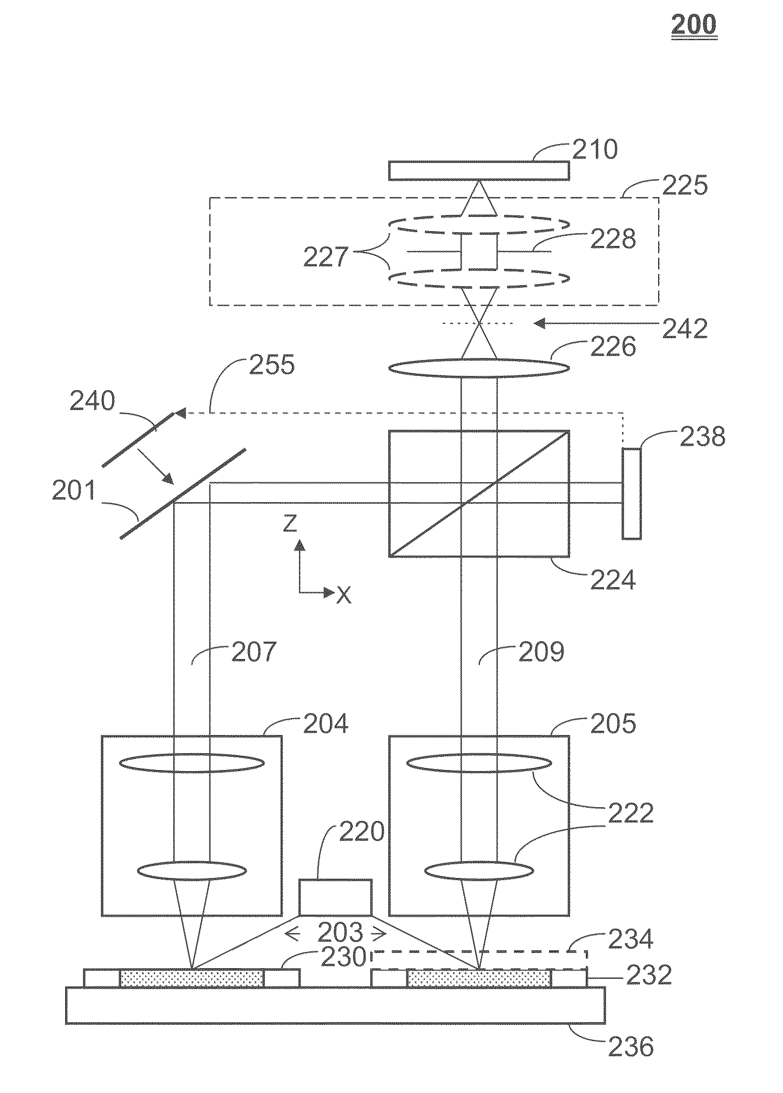
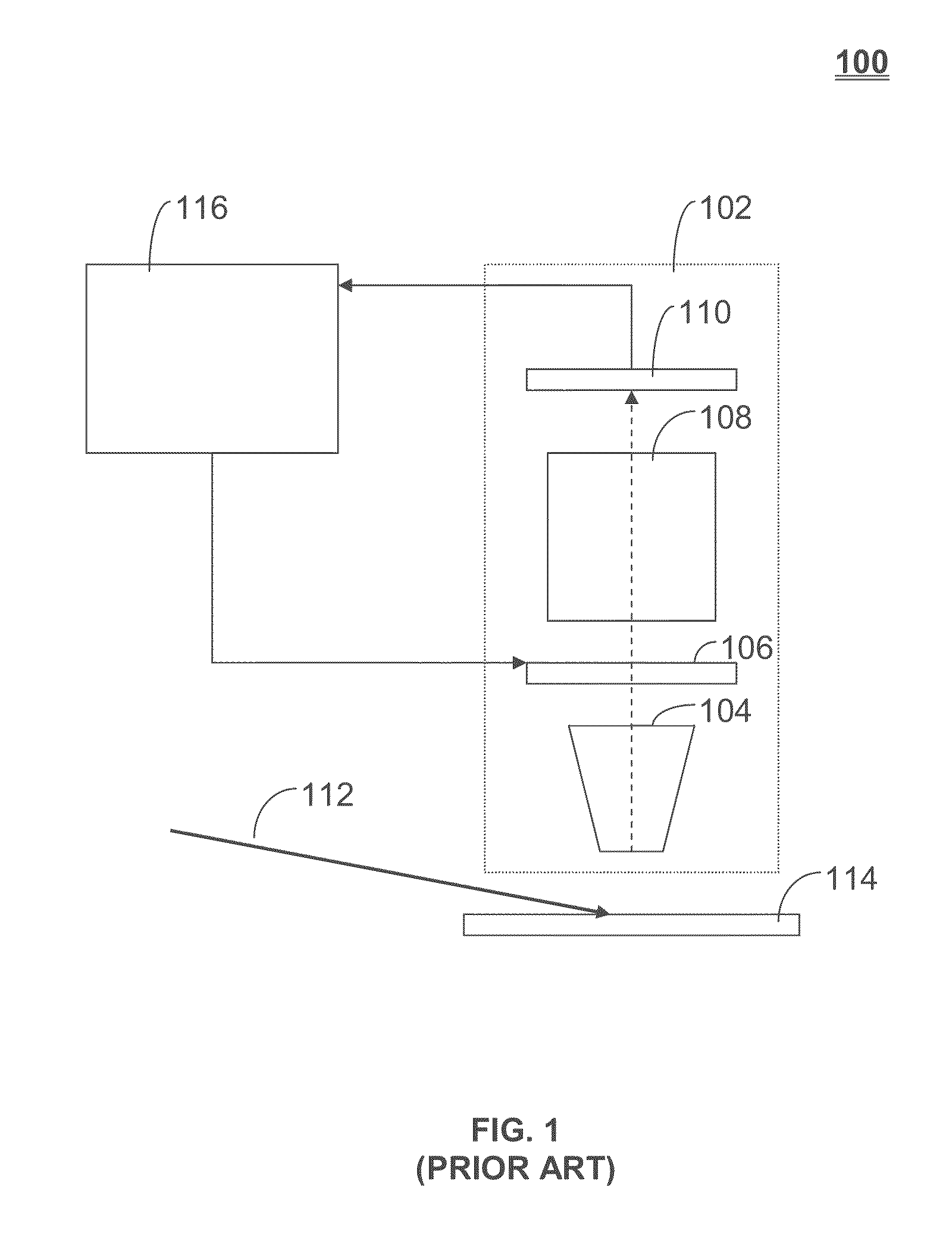
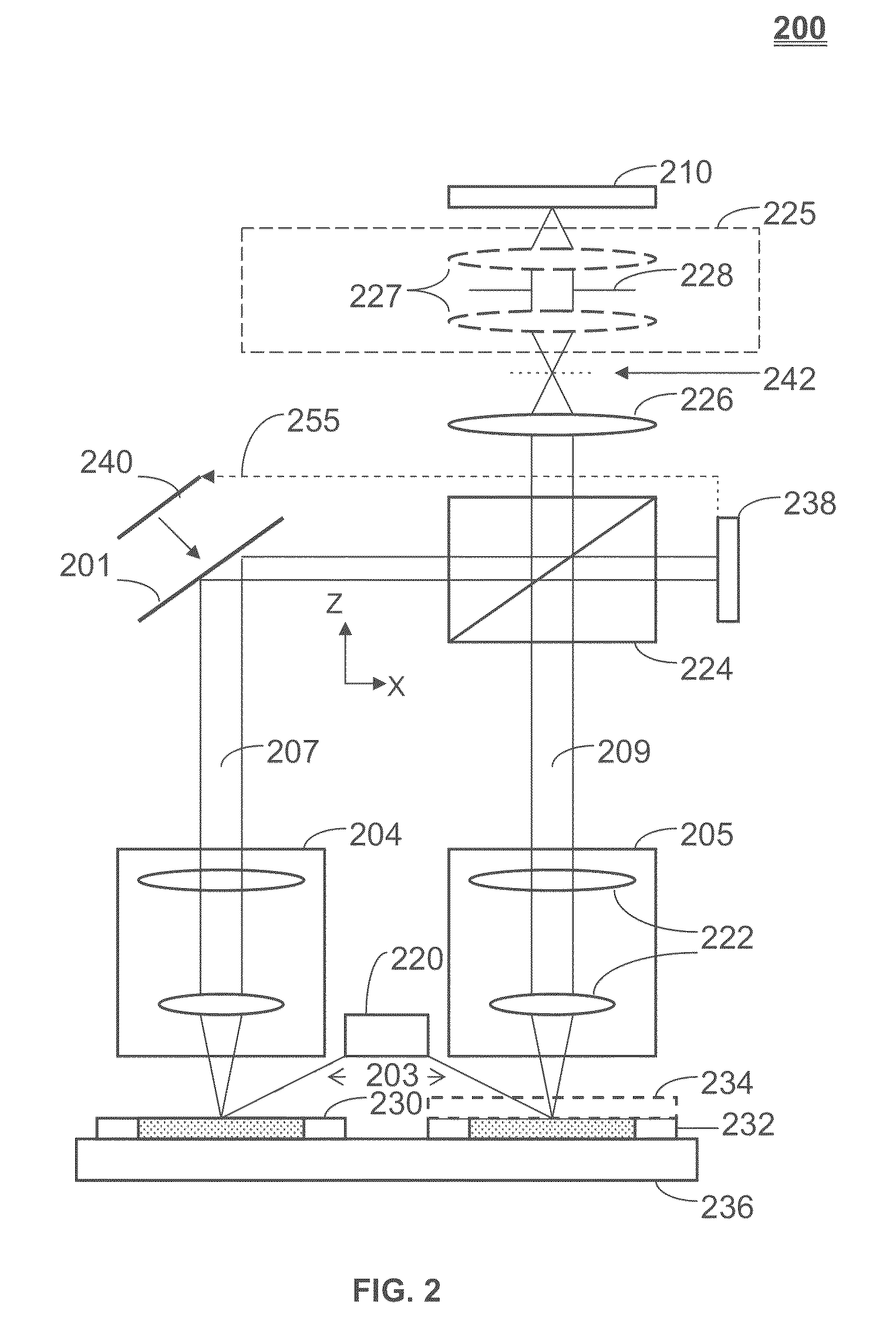

Method for detecting sub-pixel motion for optical navigation device
PatentInactiveUS7502515B2
Innovation
- The method calculates sub-pixel motion using brightness curve equations represented as functions of positional coordinates (x, y) and employs first-order derivative Taylor Expansion to generate equations for determining displacement, allowing for accurate sub-pixel motion detection without relying on a search window, and classifies and filters pixels to reduce noise.


Semiconductor Manufacturing Standards and Compliance
The semiconductor manufacturing industry operates under stringent regulatory frameworks that directly impact advanced reticle inspection methodologies. International standards organizations, including SEMI, ISO, and JEDEC, have established comprehensive guidelines governing photomask quality control and defect detection protocols. These standards mandate specific performance criteria for inspection systems, including minimum detection sensitivity, false positive rates, and measurement repeatability requirements that directly influence the selection of sub-pixel detection methods.
Current compliance frameworks require reticle inspection systems to achieve defect detection capabilities below 20nm for advanced technology nodes. The SEMI P37 standard specifically addresses photomask inspection requirements, establishing protocols for both die-to-die and die-to-database comparison methodologies. These regulations necessitate that inspection systems demonstrate consistent sub-pixel accuracy across various defect types, including phase defects, transmission variations, and geometric distortions.
Quality assurance protocols mandated by industry standards emphasize the critical importance of measurement traceability and calibration procedures. Inspection systems must undergo regular certification processes to ensure compliance with established metrology standards. The ISO 9001 quality management framework requires documented validation of inspection methodologies, including statistical process control measures and measurement uncertainty analysis for sub-pixel detection algorithms.
Regulatory compliance extends beyond technical performance to encompass data integrity and cybersecurity requirements. Modern semiconductor facilities must adhere to strict data governance protocols, ensuring that inspection results and process parameters are securely stored and traceable throughout the manufacturing lifecycle. These requirements influence the design and implementation of advanced inspection systems, necessitating robust data management capabilities alongside high-precision detection performance.
The evolving regulatory landscape continues to drive innovation in reticle inspection technologies. Emerging standards for extreme ultraviolet lithography and next-generation semiconductor devices are establishing even more demanding requirements for sub-pixel detection accuracy, pushing the boundaries of current inspection methodologies and driving the development of novel detection approaches.
Current compliance frameworks require reticle inspection systems to achieve defect detection capabilities below 20nm for advanced technology nodes. The SEMI P37 standard specifically addresses photomask inspection requirements, establishing protocols for both die-to-die and die-to-database comparison methodologies. These regulations necessitate that inspection systems demonstrate consistent sub-pixel accuracy across various defect types, including phase defects, transmission variations, and geometric distortions.
Quality assurance protocols mandated by industry standards emphasize the critical importance of measurement traceability and calibration procedures. Inspection systems must undergo regular certification processes to ensure compliance with established metrology standards. The ISO 9001 quality management framework requires documented validation of inspection methodologies, including statistical process control measures and measurement uncertainty analysis for sub-pixel detection algorithms.
Regulatory compliance extends beyond technical performance to encompass data integrity and cybersecurity requirements. Modern semiconductor facilities must adhere to strict data governance protocols, ensuring that inspection results and process parameters are securely stored and traceable throughout the manufacturing lifecycle. These requirements influence the design and implementation of advanced inspection systems, necessitating robust data management capabilities alongside high-precision detection performance.
The evolving regulatory landscape continues to drive innovation in reticle inspection technologies. Emerging standards for extreme ultraviolet lithography and next-generation semiconductor devices are establishing even more demanding requirements for sub-pixel detection accuracy, pushing the boundaries of current inspection methodologies and driving the development of novel detection approaches.
Cost-Benefit Analysis of Advanced Inspection Systems
The economic evaluation of advanced reticle inspection systems requires a comprehensive assessment of capital expenditure, operational costs, and long-term financial returns. Initial investment costs for sub-pixel quality detection systems typically range from $15-30 million per unit, depending on the inspection methodology employed. Electron beam inspection systems command premium pricing due to their superior resolution capabilities, while optical-based systems offer more moderate upfront costs but may require more frequent upgrades to maintain competitive detection sensitivity.
Operational expenditure analysis reveals significant variations across different inspection technologies. Electron beam systems incur higher maintenance costs due to complex vacuum systems and electron source replacement requirements, with annual service contracts averaging $2-3 million. Optical inspection systems demonstrate lower operational overhead but may necessitate more frequent calibration cycles and consumable replacements, particularly for advanced illumination sources and detection arrays.
The quantifiable benefits of implementing advanced inspection systems extend beyond defect detection capabilities. Yield improvement represents the primary economic driver, with sub-pixel detection enabling identification of critical defects that could otherwise propagate through the manufacturing process. Industry data indicates that advanced inspection systems can improve overall yield by 2-5%, translating to substantial revenue protection for high-volume production facilities processing thousands of wafers monthly.
Risk mitigation constitutes another crucial benefit factor, as early defect detection prevents costly downstream failures and reduces the probability of shipping defective products to customers. The cost of field failures in semiconductor applications can exceed $100,000 per incident when considering recall expenses, reputation damage, and customer relationship impacts.
Return on investment calculations typically demonstrate payback periods of 18-36 months for advanced inspection systems in high-volume manufacturing environments. Facilities processing over 10,000 wafer starts per month generally achieve faster ROI realization due to higher defect interception rates and yield improvement opportunities. The economic justification becomes particularly compelling when considering the exponential cost increase of defect detection at later manufacturing stages, where advanced inspection systems provide 10-100x cost advantage compared to post-packaging detection methods.
Operational expenditure analysis reveals significant variations across different inspection technologies. Electron beam systems incur higher maintenance costs due to complex vacuum systems and electron source replacement requirements, with annual service contracts averaging $2-3 million. Optical inspection systems demonstrate lower operational overhead but may necessitate more frequent calibration cycles and consumable replacements, particularly for advanced illumination sources and detection arrays.
The quantifiable benefits of implementing advanced inspection systems extend beyond defect detection capabilities. Yield improvement represents the primary economic driver, with sub-pixel detection enabling identification of critical defects that could otherwise propagate through the manufacturing process. Industry data indicates that advanced inspection systems can improve overall yield by 2-5%, translating to substantial revenue protection for high-volume production facilities processing thousands of wafers monthly.
Risk mitigation constitutes another crucial benefit factor, as early defect detection prevents costly downstream failures and reduces the probability of shipping defective products to customers. The cost of field failures in semiconductor applications can exceed $100,000 per incident when considering recall expenses, reputation damage, and customer relationship impacts.
Return on investment calculations typically demonstrate payback periods of 18-36 months for advanced inspection systems in high-volume manufacturing environments. Facilities processing over 10,000 wafer starts per month generally achieve faster ROI realization due to higher defect interception rates and yield improvement opportunities. The economic justification becomes particularly compelling when considering the exponential cost increase of defect detection at later manufacturing stages, where advanced inspection systems provide 10-100x cost advantage compared to post-packaging detection methods.
Unlock deeper insights with PatSnap Eureka Quick Research — get a full tech report to explore trends and direct your research. Try now!
Generate Your Research Report Instantly with AI Agent
Supercharge your innovation with PatSnap Eureka AI Agent Platform!