

Compare HBM Memory Layers for Higher Density and Efficiency
MAY 18, 20269 MIN READ
Generate Your Research Report Instantly with AI Agent
PatSnap Eureka helps you evaluate technical feasibility & market potential.
HBM Memory Evolution Background and Density Goals
High Bandwidth Memory (HBM) technology emerged from the critical need to address the growing memory bandwidth bottleneck in high-performance computing applications. The evolution began in the early 2010s when traditional memory architectures could no longer satisfy the exponential growth in data processing requirements driven by artificial intelligence, graphics processing, and scientific computing workloads.
The foundational development of HBM represented a paradigm shift from conventional planar memory designs to three-dimensional stacked architectures. This revolutionary approach leveraged through-silicon via (TSV) technology to vertically integrate multiple DRAM dies, creating a compact memory solution with significantly enhanced bandwidth capabilities. The initial HBM specification, introduced in 2013, established the groundwork for subsequent generations that would progressively increase both density and efficiency.
HBM's evolutionary trajectory has been characterized by systematic improvements in layer count, data transfer rates, and power efficiency. The first-generation HBM supported up to four memory layers with a bandwidth of 128 GB/s per stack. HBM2 expanded this capability to eight layers while doubling the bandwidth to 256 GB/s. The latest HBM3 generation pushes boundaries further, supporting up to 16 layers and achieving bandwidths exceeding 600 GB/s per stack.
The primary density goals driving HBM evolution center on maximizing memory capacity within minimal physical footprints while maintaining thermal and electrical integrity. Each additional layer in the HBM stack presents unique engineering challenges, including signal integrity maintenance, thermal management, and manufacturing yield optimization. The industry's pursuit of higher layer counts reflects the relentless demand for memory solutions that can support increasingly complex computational workloads.
Current density objectives focus on achieving optimal balance between layer count, individual die capacity, and overall system performance. The transition from 4-layer to 8-layer configurations demonstrated significant density improvements, while the progression to 12-layer and 16-layer implementations represents the cutting edge of current manufacturing capabilities. These advancements directly correlate with enhanced computational efficiency in applications ranging from machine learning accelerators to high-performance graphics processing units.
The efficiency goals encompass not only raw performance metrics but also power consumption optimization and thermal characteristics. Higher layer counts must be balanced against increased power density and heat generation, requiring sophisticated thermal management solutions and advanced packaging technologies to maintain reliable operation across diverse operating conditions.
The foundational development of HBM represented a paradigm shift from conventional planar memory designs to three-dimensional stacked architectures. This revolutionary approach leveraged through-silicon via (TSV) technology to vertically integrate multiple DRAM dies, creating a compact memory solution with significantly enhanced bandwidth capabilities. The initial HBM specification, introduced in 2013, established the groundwork for subsequent generations that would progressively increase both density and efficiency.
HBM's evolutionary trajectory has been characterized by systematic improvements in layer count, data transfer rates, and power efficiency. The first-generation HBM supported up to four memory layers with a bandwidth of 128 GB/s per stack. HBM2 expanded this capability to eight layers while doubling the bandwidth to 256 GB/s. The latest HBM3 generation pushes boundaries further, supporting up to 16 layers and achieving bandwidths exceeding 600 GB/s per stack.
The primary density goals driving HBM evolution center on maximizing memory capacity within minimal physical footprints while maintaining thermal and electrical integrity. Each additional layer in the HBM stack presents unique engineering challenges, including signal integrity maintenance, thermal management, and manufacturing yield optimization. The industry's pursuit of higher layer counts reflects the relentless demand for memory solutions that can support increasingly complex computational workloads.
Current density objectives focus on achieving optimal balance between layer count, individual die capacity, and overall system performance. The transition from 4-layer to 8-layer configurations demonstrated significant density improvements, while the progression to 12-layer and 16-layer implementations represents the cutting edge of current manufacturing capabilities. These advancements directly correlate with enhanced computational efficiency in applications ranging from machine learning accelerators to high-performance graphics processing units.
The efficiency goals encompass not only raw performance metrics but also power consumption optimization and thermal characteristics. Higher layer counts must be balanced against increased power density and heat generation, requiring sophisticated thermal management solutions and advanced packaging technologies to maintain reliable operation across diverse operating conditions.
Market Demand for High-Density HBM Solutions
The global semiconductor industry is experiencing unprecedented demand for high-bandwidth memory solutions, driven primarily by the explosive growth in artificial intelligence, machine learning, and high-performance computing applications. Data centers worldwide are rapidly expanding their processing capabilities to handle increasingly complex AI workloads, creating substantial pressure for memory technologies that can deliver both exceptional performance and space efficiency.
Cloud service providers and hyperscale data center operators represent the largest segment driving HBM demand. These organizations require memory solutions that can support massive parallel processing tasks while maintaining optimal power consumption ratios. The transition from traditional computing architectures to AI-accelerated systems has fundamentally altered memory requirements, with applications now demanding significantly higher bandwidth and lower latency than conventional DRAM solutions can provide.
The automotive sector is emerging as another critical demand driver, particularly with the advancement of autonomous driving technologies and sophisticated in-vehicle computing systems. Modern vehicles require real-time processing of vast amounts of sensor data, necessitating memory solutions that can handle multiple data streams simultaneously without compromising system responsiveness.
Graphics processing and gaming applications continue to fuel substantial market demand, with next-generation graphics cards requiring increasingly sophisticated memory architectures to support higher resolution displays, complex rendering algorithms, and immersive virtual reality experiences. Professional visualization and content creation markets similarly demand high-density memory solutions to handle large-scale 3D modeling, video editing, and scientific simulation workloads.
Edge computing deployment is creating new market opportunities for compact, high-density memory solutions. As processing capabilities migrate closer to data sources, there is growing demand for memory technologies that can deliver server-class performance within significantly constrained physical footprints.
The telecommunications infrastructure sector, particularly with 5G network deployment and future 6G development, requires memory solutions capable of handling massive data throughput while maintaining energy efficiency standards. Network equipment manufacturers are increasingly specifying high-density HBM solutions to meet stringent performance requirements within space-limited hardware configurations.
Manufacturing capacity constraints and supply chain considerations are influencing market dynamics, with customers seeking memory solutions that offer improved density to maximize performance within available silicon real estate while reducing overall system complexity and cost.
Cloud service providers and hyperscale data center operators represent the largest segment driving HBM demand. These organizations require memory solutions that can support massive parallel processing tasks while maintaining optimal power consumption ratios. The transition from traditional computing architectures to AI-accelerated systems has fundamentally altered memory requirements, with applications now demanding significantly higher bandwidth and lower latency than conventional DRAM solutions can provide.
The automotive sector is emerging as another critical demand driver, particularly with the advancement of autonomous driving technologies and sophisticated in-vehicle computing systems. Modern vehicles require real-time processing of vast amounts of sensor data, necessitating memory solutions that can handle multiple data streams simultaneously without compromising system responsiveness.
Graphics processing and gaming applications continue to fuel substantial market demand, with next-generation graphics cards requiring increasingly sophisticated memory architectures to support higher resolution displays, complex rendering algorithms, and immersive virtual reality experiences. Professional visualization and content creation markets similarly demand high-density memory solutions to handle large-scale 3D modeling, video editing, and scientific simulation workloads.
Edge computing deployment is creating new market opportunities for compact, high-density memory solutions. As processing capabilities migrate closer to data sources, there is growing demand for memory technologies that can deliver server-class performance within significantly constrained physical footprints.
The telecommunications infrastructure sector, particularly with 5G network deployment and future 6G development, requires memory solutions capable of handling massive data throughput while maintaining energy efficiency standards. Network equipment manufacturers are increasingly specifying high-density HBM solutions to meet stringent performance requirements within space-limited hardware configurations.
Manufacturing capacity constraints and supply chain considerations are influencing market dynamics, with customers seeking memory solutions that offer improved density to maximize performance within available silicon real estate while reducing overall system complexity and cost.
Current HBM Layer Stacking Challenges and Limitations
High Bandwidth Memory (HBM) layer stacking faces significant thermal management challenges that limit achievable density and efficiency. As memory layers increase, heat dissipation becomes increasingly problematic due to the vertical architecture's inherent thermal resistance. The stacked configuration creates thermal hotspots in middle layers, where heat cannot efficiently escape through conventional pathways. This thermal accumulation leads to performance throttling and reliability concerns, particularly affecting the uppermost dies that experience the highest temperatures.
Manufacturing complexity presents another critical limitation in current HBM stacking approaches. The through-silicon via (TSV) technology required for vertical interconnection becomes increasingly difficult to implement as layer count grows. TSV alignment precision requirements intensify with each additional layer, creating yield challenges that significantly impact production costs. The micro-bump bonding process between layers also faces scalability issues, as maintaining consistent electrical connections across multiple interfaces becomes exponentially more challenging.
Power delivery and signal integrity degradation represent fundamental bottlenecks in multi-layer HBM architectures. Voltage drop across multiple stacked layers creates power delivery network inefficiencies, particularly affecting the topmost memory dies. Signal propagation delays and crosstalk interference increase proportionally with layer count, limiting achievable data rates and overall system performance. The parasitic capacitance and inductance introduced by extended TSV paths further compound these electrical challenges.
Current packaging limitations constrain the practical implementation of higher-density HBM configurations. The substrate technology and interposer designs struggle to accommodate the increased complexity of multi-layer stacking while maintaining acceptable form factors. Warpage and mechanical stress issues become more pronounced with additional layers, potentially compromising long-term reliability and assembly yield.
Testing and validation complexities escalate dramatically with increased layer counts. Built-in self-test capabilities become more challenging to implement across multiple stacked dies, while failure analysis and repair mechanisms face significant accessibility constraints. These factors collectively limit the commercial viability of ultra-high-density HBM implementations, necessitating innovative solutions to overcome current technological barriers and achieve next-generation memory density targets.
Manufacturing complexity presents another critical limitation in current HBM stacking approaches. The through-silicon via (TSV) technology required for vertical interconnection becomes increasingly difficult to implement as layer count grows. TSV alignment precision requirements intensify with each additional layer, creating yield challenges that significantly impact production costs. The micro-bump bonding process between layers also faces scalability issues, as maintaining consistent electrical connections across multiple interfaces becomes exponentially more challenging.
Power delivery and signal integrity degradation represent fundamental bottlenecks in multi-layer HBM architectures. Voltage drop across multiple stacked layers creates power delivery network inefficiencies, particularly affecting the topmost memory dies. Signal propagation delays and crosstalk interference increase proportionally with layer count, limiting achievable data rates and overall system performance. The parasitic capacitance and inductance introduced by extended TSV paths further compound these electrical challenges.
Current packaging limitations constrain the practical implementation of higher-density HBM configurations. The substrate technology and interposer designs struggle to accommodate the increased complexity of multi-layer stacking while maintaining acceptable form factors. Warpage and mechanical stress issues become more pronounced with additional layers, potentially compromising long-term reliability and assembly yield.
Testing and validation complexities escalate dramatically with increased layer counts. Built-in self-test capabilities become more challenging to implement across multiple stacked dies, while failure analysis and repair mechanisms face significant accessibility constraints. These factors collectively limit the commercial viability of ultra-high-density HBM implementations, necessitating innovative solutions to overcome current technological barriers and achieve next-generation memory density targets.
Existing Multi-Layer HBM Stacking Technologies
01 Three-dimensional memory stacking architectures
Advanced three-dimensional stacking techniques enable multiple memory layers to be vertically integrated, significantly increasing memory density while maintaining compact form factors. These architectures utilize through-silicon vias and advanced packaging technologies to create high-density memory configurations with improved bandwidth and reduced footprint compared to traditional planar designs.- Three-dimensional memory stacking architectures: Advanced three-dimensional stacking techniques enable higher memory density by vertically integrating multiple memory layers within a single package. These architectures utilize through-silicon vias and advanced packaging technologies to create compact, high-capacity memory solutions that significantly increase storage density while maintaining efficient data access patterns.
- Memory layer interconnect optimization: Optimized interconnect structures between memory layers improve signal integrity and reduce power consumption while enabling faster data transfer rates. These interconnect solutions include advanced routing schemes, signal conditioning circuits, and impedance matching techniques that enhance overall memory system efficiency.
- Power management and thermal control: Sophisticated power management systems and thermal control mechanisms are essential for maintaining efficiency in high-density memory configurations. These systems include dynamic voltage scaling, temperature monitoring, and heat dissipation structures that prevent thermal throttling while optimizing power consumption across multiple memory layers.
- Memory controller and access scheduling: Advanced memory controllers implement intelligent scheduling algorithms and access optimization techniques to maximize bandwidth utilization and minimize latency in multi-layer memory systems. These controllers coordinate data flow between layers and implement predictive caching strategies to enhance overall system performance.
- Manufacturing process integration: Specialized manufacturing processes enable the integration of multiple memory layers with high yield and reliability. These processes include wafer-level packaging techniques, precision alignment systems, and quality control methods that ensure consistent performance across all memory layers while maintaining cost-effectiveness in high-volume production.
02 High-bandwidth memory interface optimization
Specialized interface designs and protocols optimize data transfer rates between memory layers and processing units. These implementations focus on minimizing latency, maximizing throughput, and ensuring efficient communication pathways through advanced signaling techniques and optimized data routing mechanisms.Expand Specific Solutions03 Memory layer interconnect technologies
Advanced interconnect solutions provide efficient electrical and thermal pathways between multiple memory layers. These technologies include innovative bonding techniques, micro-bump connections, and specialized routing architectures that enable seamless integration while maintaining signal integrity and thermal management across the memory stack.Expand Specific Solutions04 Power management and thermal control systems
Sophisticated power distribution and thermal management systems ensure optimal performance across multiple memory layers. These solutions incorporate dynamic power scaling, heat dissipation mechanisms, and temperature monitoring to maintain efficiency while preventing thermal-induced performance degradation in high-density memory configurations.Expand Specific Solutions05 Memory controller and access optimization
Advanced memory controllers implement intelligent scheduling algorithms and access patterns to maximize efficiency across multiple memory layers. These systems optimize data placement, implement predictive caching strategies, and coordinate simultaneous access operations to achieve maximum bandwidth utilization while minimizing power consumption.Expand Specific Solutions
Leading HBM Manufacturers and Market Competition
The HBM memory layers market is experiencing rapid growth driven by increasing demand for high-performance computing and AI applications. The industry is in an expansion phase with significant market potential, as data centers and AI workloads require higher memory bandwidth and capacity. Technology maturity varies significantly across players, with established leaders like Samsung Electronics, Micron Technology, and Taiwan Semiconductor Manufacturing demonstrating advanced HBM production capabilities. Memory specialists including Yangtze Memory Technologies and ChangXin Memory Technologies are developing competitive solutions, while technology giants such as Huawei Technologies and Advanced Micro Devices focus on integration and system-level optimization. The competitive landscape shows a mix of mature semiconductor manufacturers with proven HBM expertise and emerging players investing heavily in next-generation memory architectures to capture market share in this high-growth segment.
Samsung Electronics Co., Ltd.
Technical Solution: Samsung has developed advanced HBM3E technology with up to 36GB capacity per stack using 16-layer configuration, achieving 9.6 Gbps data rates and 1.2TB/s bandwidth. Their innovative through-silicon via (TSV) technology enables vertical stacking of memory dies with reduced power consumption by 20% compared to previous generations. Samsung's proprietary thermal management solutions include advanced heat spreaders and optimized die placement to maintain performance under high-density operations. The company utilizes advanced 1α (1-alpha) DRAM process technology for higher density while maintaining signal integrity across multiple layers.
Strengths: Market leadership in HBM production, proven manufacturing scalability, advanced thermal management. Weaknesses: Higher cost structure, complex manufacturing process requiring significant capital investment.
International Business Machines Corp.
Technical Solution: IBM focuses on research and development of next-generation HBM architectures, including exploration of alternative materials and novel interconnect technologies for improved density and efficiency. Their research includes advanced through-silicon via designs using copper-filled TSVs with reduced resistance and improved thermal conductivity. IBM investigates hybrid memory architectures combining HBM with emerging memory technologies like phase-change memory for enhanced performance characteristics. The company's work on 3D memory architectures includes innovative stacking methodologies and advanced error correction schemes for ultra-high-density configurations. Their thermal management research focuses on micro-channel cooling and advanced thermal interface materials for next-generation HBM implementations.
Strengths: Strong research capabilities, innovative architectural approaches, advanced materials research expertise. Weaknesses: Limited commercial manufacturing presence, longer development cycles for technology transfer to production.
Core Patents in HBM Layer Integration Methods
Device Disaggregation For Improved Performance
PatentPendingUS20240234424A1
Innovation
- A 3D semiconductor device architecture is implemented, combining an active die in an advanced node with a passive die in a legacy node, featuring dense interconnects and multiplexers, allowing for high bandwidth and reduced latency through face-to-face or back-to-back bonding of tiers with through-silicon vias, and utilizing a repeating pattern of data, power, and ground interconnects.
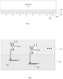
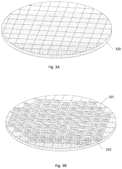
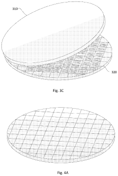
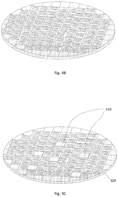
High speed memory interface
PatentActiveUS10467177B2
Innovation
- The Enhanced HBM (EHBM) interface reduces the number of physical wires while operating at higher signaling rates, using Kandou CNRZ-5 channels and orthogonal differential vector signaling to efficiently transmit data over a narrower interface, allowing for lower-cost organic interposers and reduced pin count, while maintaining high bandwidth and low latency.


Thermal Management in High-Density HBM Stacks
Thermal management represents one of the most critical engineering challenges in high-density HBM stack implementations, directly impacting both performance sustainability and reliability. As HBM architectures evolve toward higher layer counts and increased data throughput, the thermal density within these compact memory modules intensifies exponentially, creating localized hotspots that can severely degrade performance and reduce component lifespan.
The fundamental thermal challenge stems from the vertical stacking architecture inherent to HBM design. Unlike traditional planar memory configurations, HBM stacks concentrate multiple DRAM dies within a confined three-dimensional space, creating significant heat generation density. Each additional layer contributes to cumulative thermal buildup, with the central layers experiencing the most severe thermal stress due to limited heat dissipation pathways.
Advanced thermal interface materials have emerged as a primary solution for managing interlayer heat transfer. These specialized materials, including graphene-enhanced thermal pads and liquid metal interfaces, provide superior thermal conductivity compared to conventional solutions. The selection of appropriate thermal interface materials directly influences the thermal resistance between layers and the overall thermal gradient across the stack.
Through-silicon via design optimization plays a crucial role in thermal management strategy. Beyond their primary function of electrical connectivity, TSVs can be strategically designed and positioned to serve as thermal conduits, facilitating heat transfer from internal layers to external surfaces where conventional cooling solutions can be more effectively applied.
Package-level thermal solutions have evolved to address the unique challenges of HBM thermal management. Integrated heat spreaders, micro-channel cooling systems, and advanced substrate materials work in conjunction to create comprehensive thermal management ecosystems. These solutions must balance thermal performance with the stringent space constraints and electrical requirements of high-density memory applications.
Thermal monitoring and dynamic management systems represent an emerging approach to maintaining optimal operating temperatures. Real-time temperature sensing integrated within HBM stacks enables adaptive performance scaling and thermal throttling mechanisms, ensuring sustained operation within safe thermal envelopes while maximizing performance during favorable thermal conditions.
The fundamental thermal challenge stems from the vertical stacking architecture inherent to HBM design. Unlike traditional planar memory configurations, HBM stacks concentrate multiple DRAM dies within a confined three-dimensional space, creating significant heat generation density. Each additional layer contributes to cumulative thermal buildup, with the central layers experiencing the most severe thermal stress due to limited heat dissipation pathways.
Advanced thermal interface materials have emerged as a primary solution for managing interlayer heat transfer. These specialized materials, including graphene-enhanced thermal pads and liquid metal interfaces, provide superior thermal conductivity compared to conventional solutions. The selection of appropriate thermal interface materials directly influences the thermal resistance between layers and the overall thermal gradient across the stack.
Through-silicon via design optimization plays a crucial role in thermal management strategy. Beyond their primary function of electrical connectivity, TSVs can be strategically designed and positioned to serve as thermal conduits, facilitating heat transfer from internal layers to external surfaces where conventional cooling solutions can be more effectively applied.
Package-level thermal solutions have evolved to address the unique challenges of HBM thermal management. Integrated heat spreaders, micro-channel cooling systems, and advanced substrate materials work in conjunction to create comprehensive thermal management ecosystems. These solutions must balance thermal performance with the stringent space constraints and electrical requirements of high-density memory applications.
Thermal monitoring and dynamic management systems represent an emerging approach to maintaining optimal operating temperatures. Real-time temperature sensing integrated within HBM stacks enables adaptive performance scaling and thermal throttling mechanisms, ensuring sustained operation within safe thermal envelopes while maximizing performance during favorable thermal conditions.
Power Efficiency Standards for Advanced HBM
Power efficiency has emerged as a critical performance metric for advanced High Bandwidth Memory (HBM) architectures, particularly as memory systems scale to support increasingly demanding computational workloads. The establishment of comprehensive power efficiency standards becomes essential for evaluating and optimizing HBM implementations across different layer configurations and operational scenarios.
Current power efficiency standards for HBM focus on several key metrics, including power consumption per gigabyte per second (pJ/bit), idle power consumption, and dynamic power scaling capabilities. Industry organizations such as JEDEC have established baseline power consumption guidelines, with HBM3 specifications targeting power efficiency improvements of 20-30% compared to previous generations. These standards define maximum power consumption limits ranging from 15-20 watts for standard HBM3 implementations, with enhanced variants allowing up to 30 watts for high-performance applications.
The measurement methodologies for power efficiency encompass both static and dynamic power consumption patterns. Static power measurements evaluate leakage current and standby power consumption across different voltage domains, while dynamic measurements assess power consumption during various memory access patterns, including sequential reads, random access operations, and burst transfers. Temperature-dependent power scaling requirements are also incorporated into these standards to ensure consistent performance across operational temperature ranges.
Advanced HBM power efficiency standards introduce sophisticated power management features, including per-bank power gating, adaptive voltage scaling, and intelligent refresh rate optimization. These features enable fine-grained power control that can reduce overall system power consumption by 15-25% during typical workloads. The standards also define power state transition timings and minimum retention voltages to ensure data integrity during power management operations.
Compliance testing protocols for power efficiency standards involve comprehensive validation across multiple operational scenarios, including peak performance conditions, typical workload patterns, and low-power standby modes. These protocols ensure that HBM implementations meet both performance and power consumption requirements while maintaining reliability and data integrity standards essential for mission-critical applications.
Current power efficiency standards for HBM focus on several key metrics, including power consumption per gigabyte per second (pJ/bit), idle power consumption, and dynamic power scaling capabilities. Industry organizations such as JEDEC have established baseline power consumption guidelines, with HBM3 specifications targeting power efficiency improvements of 20-30% compared to previous generations. These standards define maximum power consumption limits ranging from 15-20 watts for standard HBM3 implementations, with enhanced variants allowing up to 30 watts for high-performance applications.
The measurement methodologies for power efficiency encompass both static and dynamic power consumption patterns. Static power measurements evaluate leakage current and standby power consumption across different voltage domains, while dynamic measurements assess power consumption during various memory access patterns, including sequential reads, random access operations, and burst transfers. Temperature-dependent power scaling requirements are also incorporated into these standards to ensure consistent performance across operational temperature ranges.
Advanced HBM power efficiency standards introduce sophisticated power management features, including per-bank power gating, adaptive voltage scaling, and intelligent refresh rate optimization. These features enable fine-grained power control that can reduce overall system power consumption by 15-25% during typical workloads. The standards also define power state transition timings and minimum retention voltages to ensure data integrity during power management operations.
Compliance testing protocols for power efficiency standards involve comprehensive validation across multiple operational scenarios, including peak performance conditions, typical workload patterns, and low-power standby modes. These protocols ensure that HBM implementations meet both performance and power consumption requirements while maintaining reliability and data integrity standards essential for mission-critical applications.
Unlock deeper insights with PatSnap Eureka Quick Research — get a full tech report to explore trends and direct your research. Try now!
Generate Your Research Report Instantly with AI Agent
Supercharge your innovation with PatSnap Eureka AI Agent Platform!