

Comparing Optical Backplane Effectiveness in AI vs ML Computational Loads
MAY 20, 20269 MIN READ
Generate Your Research Report Instantly with AI Agent
PatSnap Eureka helps you evaluate technical feasibility & market potential.
Optical Backplane AI/ML Background and Objectives
Optical backplane technology has emerged as a critical infrastructure component in modern high-performance computing systems, representing a paradigm shift from traditional electrical interconnects to photonic-based data transmission. This technology leverages optical signals to facilitate high-speed, low-latency communication between processing units, memory modules, and other system components within computing architectures.
The evolution of optical backplanes stems from the increasing demands of data-intensive applications, particularly in artificial intelligence and machine learning domains. Traditional copper-based electrical backplanes face fundamental limitations in bandwidth, power consumption, and signal integrity as data rates continue to escalate. Optical solutions address these constraints by offering superior bandwidth density, reduced electromagnetic interference, and enhanced scalability for next-generation computing platforms.
The distinction between AI and ML computational workloads presents unique challenges for interconnect design. AI applications, encompassing deep learning neural networks and real-time inference tasks, typically require massive parallel processing with intensive data movement between GPU clusters and memory hierarchies. These workloads exhibit burst-intensive communication patterns with varying latency sensitivity depending on the specific application domain.
Machine learning computational loads, while overlapping with AI in some aspects, often involve different data access patterns and processing requirements. Traditional ML algorithms may emphasize iterative computations with more predictable communication flows, whereas modern deep learning approaches demand dynamic resource allocation and adaptive bandwidth management across distributed computing nodes.
The primary objective of comparing optical backplane effectiveness across these computational paradigms involves evaluating performance metrics including throughput efficiency, latency characteristics, power consumption profiles, and scalability potential. Understanding how optical interconnect architectures respond to different traffic patterns, data locality requirements, and synchronization demands becomes essential for optimizing system-level performance.
Current research focuses on developing adaptive optical backplane solutions that can dynamically adjust to varying computational workload characteristics. This includes investigating wavelength division multiplexing techniques, optical switching mechanisms, and hybrid electro-optical architectures that maximize efficiency across diverse AI and ML application scenarios while maintaining cost-effectiveness and reliability standards.
Market Demand for AI/ML Optical Interconnect Solutions
The global AI and ML infrastructure market is experiencing unprecedented growth, driven by the exponential increase in computational demands across diverse industries. Organizations are rapidly adopting AI-driven applications ranging from autonomous vehicles and real-time fraud detection to large language models and computer vision systems. This surge has created substantial pressure on existing data center architectures, particularly in terms of interconnect bandwidth and latency requirements.
Traditional electrical interconnects are increasingly inadequate for handling the massive data throughput required by modern AI workloads. The bandwidth limitations of copper-based solutions, combined with their power consumption and heat generation issues, have created a significant market opportunity for optical interconnect technologies. Data centers processing AI inference tasks require sustained high-bandwidth communication between processing units, while ML training workloads demand even more intensive interconnect performance due to frequent parameter synchronization across distributed computing nodes.
Enterprise adoption patterns reveal distinct requirements between AI and ML applications. AI inference workloads, particularly those supporting real-time applications like autonomous driving systems and financial trading platforms, prioritize ultra-low latency optical solutions. These applications cannot tolerate the microsecond delays inherent in electrical switching systems. Conversely, ML training environments focus on maximizing aggregate bandwidth to support large-scale distributed computing frameworks, where optical backplanes can provide the necessary scalability.
Cloud service providers represent the largest segment driving optical interconnect demand, as they scale infrastructure to support both internal AI development and customer-facing ML services. The hyperscale data center market has become particularly receptive to optical backplane solutions that can reduce power consumption while increasing computational density. Edge computing deployments are emerging as another significant demand driver, where space constraints and power efficiency requirements make optical interconnects increasingly attractive.
Market dynamics indicate strong growth potential across multiple vertical sectors. Healthcare organizations implementing AI-powered diagnostic systems, financial institutions deploying real-time risk assessment algorithms, and manufacturing companies integrating predictive maintenance solutions all contribute to expanding market demand. The telecommunications industry's deployment of AI-enhanced network optimization further amplifies the need for high-performance optical interconnect solutions capable of supporting both AI inference and ML model training workloads simultaneously.
Current Optical Backplane Challenges in AI/ML Workloads
Optical backplane technology faces significant challenges when deployed in AI and ML computational environments, primarily due to the distinct characteristics of these workloads. The fundamental issue stems from the different data flow patterns and computational requirements between AI inference tasks and traditional ML training processes.
Bandwidth scalability represents a critical challenge as AI workloads, particularly large language models and computer vision applications, demand unprecedented data throughput rates. Current optical backplane architectures struggle to maintain consistent performance when handling the massive parallel data streams typical in AI inference scenarios. The situation becomes more complex with ML training workloads that require frequent parameter updates and gradient synchronization across distributed computing nodes.
Latency sensitivity poses another substantial obstacle, especially for real-time AI applications. Optical backplanes must minimize signal propagation delays while managing the conversion overhead between optical and electrical domains. This challenge is amplified in AI workloads where microsecond-level latencies can significantly impact overall system performance, particularly in edge computing scenarios requiring immediate response times.
Power efficiency constraints create additional complexity as optical transceivers and switching components consume considerable energy during high-frequency operations. AI computational loads often involve sustained high-intensity processing, leading to thermal management issues that can degrade optical component performance and reliability over extended operational periods.
Signal integrity degradation emerges as workload intensity increases, with optical backplanes experiencing crosstalk, dispersion, and attenuation issues under heavy AI/ML traffic loads. The problem intensifies when handling mixed workload scenarios where AI inference and ML training tasks compete for backplane resources simultaneously.
Protocol compatibility challenges arise from the diverse communication requirements of AI frameworks versus traditional ML algorithms. Current optical backplane designs often lack the flexibility to efficiently handle the varied message sizes, communication patterns, and synchronization requirements inherent in different AI/ML computational paradigms.
Cost-performance optimization remains problematic as organizations struggle to justify the high implementation costs of advanced optical backplane solutions against the performance gains achieved in specific AI/ML workload scenarios. This economic challenge is particularly acute for smaller organizations seeking to deploy AI capabilities without substantial infrastructure investments.
Current AI vs ML Optical Backplane Solutions
01 Optical signal transmission and routing in backplane systems
Technologies for transmitting and routing optical signals within backplane architectures to improve data communication effectiveness. These systems utilize optical pathways and switching mechanisms to direct light-based signals between different components and modules within the backplane infrastructure, enabling high-speed data transfer with reduced latency and improved signal integrity.- Optical signal transmission and routing in backplane systems: Technologies for transmitting and routing optical signals within backplane architectures to improve data communication efficiency. These systems utilize optical pathways and switching mechanisms to direct light-based signals between different components and modules within the backplane infrastructure.
- Optical coupling and connection mechanisms: Methods and devices for establishing reliable optical connections between components in backplane systems. These mechanisms ensure proper alignment and coupling of optical elements to minimize signal loss and maintain high transmission quality across the backplane network.
- Signal processing and amplification techniques: Advanced signal processing methods to enhance optical signal quality and strength within backplane systems. These techniques include amplification, filtering, and conditioning of optical signals to maintain signal integrity over longer distances and through multiple connections.
- Optical backplane architecture and design optimization: Structural designs and architectural approaches for optimizing optical backplane performance. These solutions focus on the physical layout, component arrangement, and system integration to maximize throughput while minimizing interference and cross-talk between optical channels.
- Performance monitoring and control systems: Systems for monitoring and controlling the performance of optical backplane networks. These solutions provide real-time assessment of signal quality, system health, and operational parameters to ensure optimal performance and enable predictive maintenance of the optical infrastructure.
02 Optical connector and coupling mechanisms for backplane interfaces
Design and implementation of optical connectors and coupling systems that facilitate effective optical connections in backplane environments. These mechanisms ensure proper alignment and coupling of optical signals between different backplane components, maintaining signal quality and minimizing losses during transmission across the optical backplane network.Expand Specific Solutions03 Optical waveguide integration and fabrication in backplane structures
Methods for integrating and fabricating optical waveguides directly into backplane substrates to enhance optical signal propagation effectiveness. These approaches involve embedding or constructing optical pathways within the backplane material itself, creating integrated optical circuits that provide efficient light transmission with minimal signal degradation and crosstalk.Expand Specific Solutions04 Optical switching and multiplexing for backplane data management
Implementation of optical switching and multiplexing technologies to manage and control data flow within backplane systems. These solutions enable dynamic routing of optical signals, wavelength division multiplexing, and switching capabilities that optimize bandwidth utilization and improve overall system performance in high-density backplane configurations.Expand Specific Solutions05 Optical power distribution and signal amplification in backplane networks
Systems for distributing optical power and amplifying signals throughout backplane networks to maintain signal strength and quality across extended distances. These technologies include optical amplifiers, power splitters, and signal conditioning components that ensure consistent optical signal levels and compensate for transmission losses within the backplane infrastructure.Expand Specific Solutions
Key Players in Optical Backplane and AI/ML Infrastructure
The optical backplane technology for AI versus ML computational loads represents an emerging market segment within the broader high-performance computing infrastructure industry. The market is currently in its early growth phase, driven by increasing demand for faster data processing and reduced latency in AI/ML applications. Market size remains relatively niche but expanding rapidly as enterprises scale their AI operations. Technology maturity varies significantly across players, with established semiconductor companies like Intel Corp., Taiwan Semiconductor Manufacturing Co., and IBM leading in foundational technologies, while display technology specialists such as BOE Technology Group, Innolux Corp., and TCL China Star provide critical optical components. Research institutions like Tsinghua University and Huazhong University of Science & Technology contribute to advancing optical interconnect innovations. Companies like Shanghai Xizhi Technology specifically focus on optical computing solutions, indicating growing specialization in this space.
Taiwan Semiconductor Manufacturing Co., Ltd.
Technical Solution: TSMC provides foundry services for optical backplane components, specializing in manufacturing silicon photonic devices using advanced semiconductor processes. Their technology enables the production of integrated optical transceivers and modulators optimized for AI/ML computational environments. TSMC's manufacturing capabilities support the creation of high-density optical interconnects with precise wavelength control and minimal crosstalk, essential for maintaining signal integrity in intensive computational workloads. Their process technology allows for the integration of electronic and photonic components on the same substrate, reducing packaging complexity and improving overall system performance for both AI training and ML inference applications.
Strengths: Leading-edge manufacturing processes, high yield rates, strong supply chain reliability. Weaknesses: Limited direct system integration capabilities, dependency on customer design expertise, high minimum order quantities.
International Business Machines Corp.
Technical Solution: IBM's optical backplane technology focuses on coherent optical transmission systems designed for high-performance computing environments. Their approach utilizes advanced modulation formats and digital signal processing to optimize data transmission for both AI and ML workloads. IBM's optical interconnects feature adaptive equalization algorithms that dynamically adjust to different computational patterns, providing up to 400 Gbps per wavelength with ultra-low latency characteristics. The system incorporates machine learning algorithms to predict traffic patterns and optimize optical path allocation, particularly effective for large-scale AI training clusters where communication overhead significantly impacts performance.
Strengths: Advanced signal processing capabilities, strong research foundation, excellent integration with enterprise systems. Weaknesses: Higher cost structure, complex deployment requirements, limited availability in consumer markets.
Core Optical Backplane Patents for AI/ML Applications
Optical backplane connector, photoelectric conversion module and optical backplane
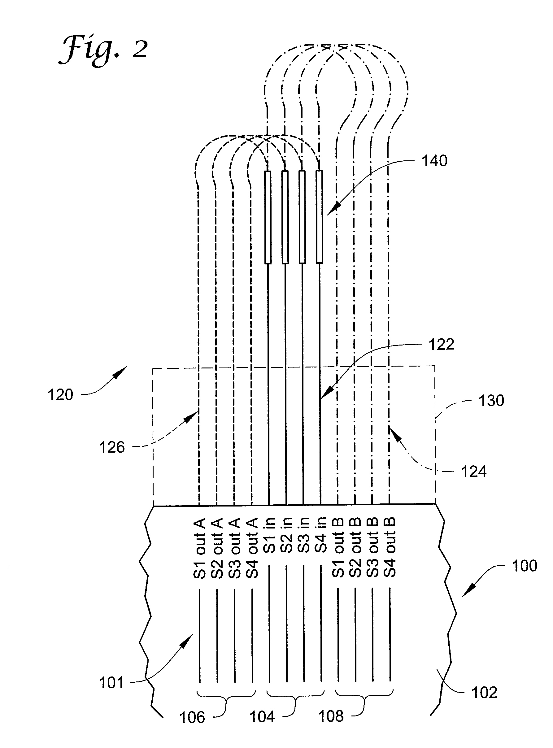
PatentInactiveUS8172467B2
Innovation
- The optical backplane connector accommodates photoelectric conversion modules with electric contacts, featuring a depression for module fitting and an elastic member for secure optical coupling, allowing for easy replacement and improved positioning accuracy, enabling higher parts density and efficient signal transmission up to 10 Gigabits per second.


Integrated functionality in optical backplane
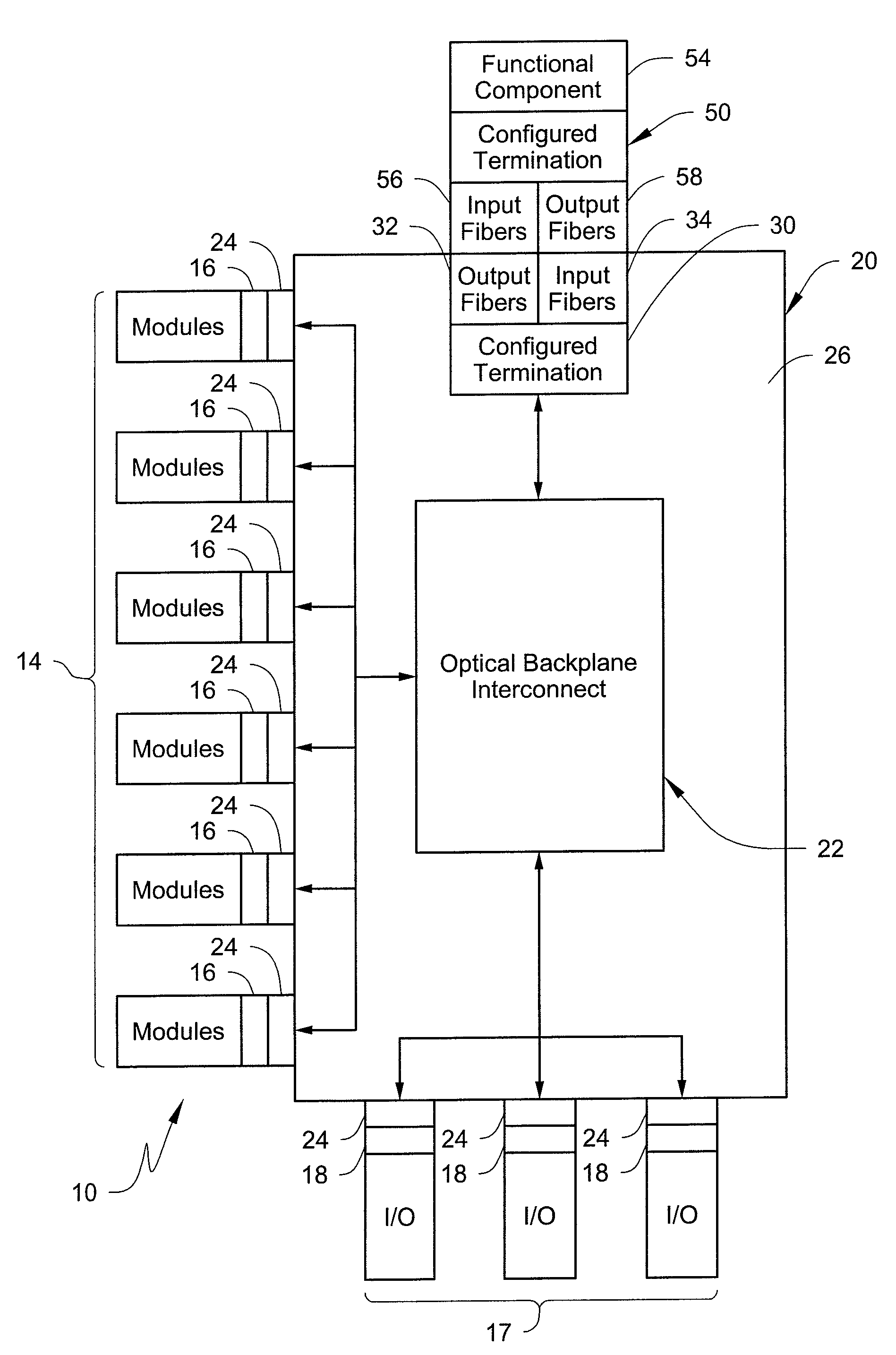
PatentInactiveUS7587115B1
Innovation
- The integration of functional optical devices with a fixed configuration of input and output fibers, fusion spliced into the optical backplane interconnect, allowing for passive or active components like splitters, attenuators, or switches to be seamlessly integrated, reducing manufacturing costs and optical loss.

Energy Efficiency Standards for Optical Computing Systems
The establishment of comprehensive energy efficiency standards for optical computing systems has become increasingly critical as these technologies transition from research laboratories to commercial deployment. Current industry initiatives focus on developing standardized metrics that can accurately measure and compare the energy performance of optical backplanes across different computational workloads, particularly in AI and ML applications.
International standards organizations, including IEEE and IEC, are actively working to define power consumption measurement protocols specifically tailored for optical computing architectures. These emerging standards address the unique characteristics of photonic systems, such as laser power requirements, thermal management needs, and the energy overhead associated with electro-optical conversions. The standards framework encompasses both static power consumption during idle states and dynamic power scaling under varying computational loads.
A key challenge in standardization lies in establishing fair comparison methodologies between optical and electronic systems. Traditional metrics like FLOPS per watt require adaptation to account for the fundamentally different operational principles of optical computing. New composite metrics are being developed that consider factors such as data throughput per joule, latency-adjusted energy efficiency, and thermal dissipation characteristics specific to photonic processing units.
The standards also address testing methodologies for different workload types, recognizing that AI inference tasks exhibit different energy profiles compared to ML training operations. Standardized benchmark suites are being developed to ensure consistent evaluation across various optical backplane implementations, enabling meaningful performance comparisons between different vendor solutions.
Compliance frameworks are emerging that define minimum energy efficiency thresholds for optical computing systems in data center environments. These standards incorporate considerations for cooling requirements, power supply efficiency, and system-level energy management, providing a holistic approach to evaluating the environmental impact of optical computing deployments in large-scale computational infrastructure.
Thermal Management in High-Performance Optical Backplanes
Thermal management represents one of the most critical engineering challenges in high-performance optical backplanes, particularly when supporting intensive AI and ML computational workloads. The fundamental issue stems from the inherent heat generation in optical components, including laser diodes, photodetectors, and optical modulators, which can significantly impact system performance and reliability if not properly addressed.
The primary heat sources in optical backplanes include active optical components such as vertical-cavity surface-emitting lasers (VCSELs), distributed feedback lasers, and high-speed photodiodes. These components generate substantial thermal energy during operation, with power densities often exceeding 10 watts per square centimeter in dense configurations. Additionally, electronic driver circuits and transimpedance amplifiers contribute to the overall thermal load, creating localized hot spots that can degrade optical performance.
Temperature variations directly affect the wavelength stability of laser sources, with typical wavelength drift rates of 0.1 nanometers per degree Celsius for standard semiconductor lasers. This thermal sensitivity becomes particularly problematic in wavelength division multiplexing systems where precise channel spacing is essential. Furthermore, elevated temperatures reduce the quantum efficiency of photodetectors and increase dark current, leading to degraded signal-to-noise ratios and higher bit error rates.
Advanced thermal management strategies for optical backplanes incorporate multi-layered approaches combining passive and active cooling techniques. Passive solutions include optimized heat sink designs with enhanced surface area, thermal interface materials with high conductivity coefficients exceeding 5 W/mK, and strategic component placement to minimize thermal coupling between adjacent elements.
Active cooling implementations utilize micro-channel liquid cooling systems, thermoelectric coolers, and forced air convection with precisely controlled airflow patterns. These systems maintain component temperatures within optimal operating ranges, typically below 70°C for commercial-grade optical devices and below 85°C for industrial applications.
Emerging thermal management innovations focus on integrated cooling solutions embedded directly within the optical backplane substrate. These include embedded heat pipes, phase-change materials for thermal buffering, and advanced thermal interface materials incorporating carbon nanotubes or graphene structures. Such approaches enable more compact designs while maintaining superior thermal performance essential for next-generation high-density optical interconnect systems.
Unlock deeper insights with PatSnap Eureka Quick Research — get a full tech report to explore trends and direct your research. Try now!
Generate Your Research Report Instantly with AI Agent
Supercharge your innovation with PatSnap Eureka AI Agent Platform!