

Reducing Signal Errors in Optical Backplanes Through Optimized Path Guides
MAY 20, 20269 MIN READ
Generate Your Research Report Instantly with AI Agent
PatSnap Eureka helps you evaluate technical feasibility & market potential.
Optical Backplane Signal Error Background and Objectives
Optical backplanes represent a critical infrastructure component in modern high-performance computing systems, data centers, and telecommunications equipment. These systems facilitate high-speed data transmission between multiple circuit boards within a single chassis or rack, replacing traditional electrical interconnects with optical pathways to overcome bandwidth limitations and signal degradation issues inherent in copper-based solutions.
The evolution of optical backplane technology has been driven by the exponential growth in data processing requirements and the need for faster, more reliable inter-board communication. Early implementations in the 1990s focused on basic point-to-point optical connections, while contemporary systems now support complex multi-gigabit architectures capable of handling terabit-scale data flows across dozens of interconnected boards.
Signal integrity remains the paramount challenge in optical backplane design, where even minor deviations in optical path geometry can result in significant data transmission errors. These errors manifest as increased bit error rates, signal attenuation, and crosstalk between adjacent channels, ultimately compromising system performance and reliability. The complexity increases exponentially in dense configurations where hundreds of optical channels must coexist within confined spaces.
Path guides serve as the fundamental mechanism for maintaining optical signal quality by precisely controlling light propagation through the backplane medium. Traditional path guide designs often suffer from manufacturing tolerances, thermal expansion effects, and mechanical stress-induced deformations that introduce unwanted signal distortions. These factors contribute to modal dispersion, insertion losses, and reflection-induced noise that degrade overall system performance.
The primary objective of optimizing path guides centers on minimizing signal errors through enhanced geometric precision, improved material selection, and advanced manufacturing techniques. This involves developing path guide architectures that maintain consistent refractive index profiles, reduce surface roughness effects, and provide superior mechanical stability under varying environmental conditions.
Secondary objectives include achieving scalable manufacturing processes that can accommodate increasing channel densities while maintaining cost-effectiveness. The optimization must also address thermal management considerations, as temperature variations can significantly impact optical path characteristics and introduce additional sources of signal degradation.
The ultimate goal encompasses establishing robust design methodologies that enable predictable signal performance across diverse operating conditions, supporting the next generation of high-bandwidth optical backplane systems required for emerging applications in artificial intelligence, cloud computing, and advanced telecommunications infrastructure.
Market Demand for High-Performance Optical Backplane Systems
The global optical backplane market is experiencing unprecedented growth driven by the exponential increase in data traffic and the proliferation of high-bandwidth applications. Data centers, telecommunications infrastructure, and high-performance computing systems are demanding increasingly sophisticated optical interconnect solutions to handle massive data throughput requirements. The shift toward cloud computing, artificial intelligence, and machine learning applications has created an urgent need for optical backplane systems that can deliver superior signal integrity and minimal transmission errors.
Enterprise data centers represent the largest market segment for high-performance optical backplane systems, as organizations struggle to maintain network performance while scaling their infrastructure. The demand is particularly acute in hyperscale data centers operated by major cloud service providers, where even minor signal degradation can result in significant performance bottlenecks and operational costs. Financial services, healthcare, and scientific research institutions also constitute substantial market segments due to their requirements for ultra-reliable, high-speed data transmission.
Telecommunications service providers are increasingly adopting optical backplane technologies to support next-generation network architectures, including 5G infrastructure and edge computing deployments. The transition from traditional copper-based backplanes to optical solutions is accelerating as network operators seek to overcome bandwidth limitations and signal integrity challenges inherent in legacy systems. This migration is creating substantial opportunities for advanced optical backplane solutions that can minimize signal errors through optimized design approaches.
The market demand is further intensified by the growing complexity of modern electronic systems, where traditional electrical backplanes face fundamental physical limitations. Signal crosstalk, electromagnetic interference, and power consumption concerns are driving system architects to seek optical alternatives that can maintain signal quality over longer distances and higher frequencies. Manufacturing sectors requiring real-time data processing and industrial automation are also contributing to market expansion.
Emerging applications in autonomous vehicles, smart cities, and Internet of Things deployments are creating new market opportunities for compact, high-performance optical backplane systems. These applications demand robust signal transmission capabilities in challenging environmental conditions, making optimized path guide designs essential for maintaining system reliability and performance standards across diverse operational scenarios.
Current Signal Error Challenges in Optical Backplane Path Guides
Optical backplane systems face significant signal integrity challenges that directly impact data transmission reliability and system performance. Signal errors in these systems primarily stem from optical path discontinuities, misalignment issues, and environmental factors that degrade signal quality during propagation through the backplane infrastructure.
Crosstalk represents one of the most persistent challenges in optical backplane path guides. Adjacent optical channels can experience unwanted signal coupling due to insufficient isolation between waveguides or inadequate shielding mechanisms. This phenomenon becomes particularly problematic in high-density configurations where multiple optical paths are routed in close proximity, leading to signal degradation and increased bit error rates.
Modal dispersion issues plague multimode optical backplane systems, where different light modes travel at varying velocities through the same waveguide. This temporal spreading of optical pulses causes intersymbol interference, limiting the maximum achievable data rates and transmission distances. The problem is exacerbated by manufacturing tolerances and variations in refractive index profiles across the backplane substrate.
Insertion loss variability across different optical paths creates significant challenges for system designers. Non-uniform losses between channels result in power imbalances that can overwhelm receiver dynamic ranges or fall below sensitivity thresholds. These variations often arise from manufacturing inconsistencies, connector interface imperfections, and material property variations within the backplane structure.
Reflection-induced signal degradation occurs at optical interfaces throughout the backplane system. Impedance mismatches at connector points, waveguide transitions, and material boundaries create back-reflections that interfere with forward-propagating signals. These reflections can cause signal distortion, reduce signal-to-noise ratios, and create timing jitter that compromises overall system performance.
Temperature-induced signal variations present ongoing operational challenges. Thermal expansion and contraction of backplane materials cause mechanical stress on optical components, leading to alignment drift and coupling efficiency variations. Additionally, temperature-dependent refractive index changes alter the optical path characteristics, causing wavelength-dependent losses and phase variations that degrade signal quality over time.
Existing Path Guide Optimization Solutions for Error Reduction
01 Error detection and correction mechanisms in optical backplanes
Implementation of advanced error detection and correction algorithms specifically designed for optical communication systems. These mechanisms include forward error correction codes, parity checking, and cyclic redundancy checks to identify and correct signal errors that occur during optical data transmission. The systems employ sophisticated encoding and decoding techniques to maintain signal integrity and reduce bit error rates in high-speed optical backplane communications.- Error detection and correction mechanisms in optical backplanes: Implementation of sophisticated error detection and correction algorithms to identify and rectify signal errors in optical backplane systems. These mechanisms include forward error correction, parity checking, and cyclic redundancy checks to ensure data integrity during optical signal transmission. The systems employ real-time monitoring and automatic correction capabilities to maintain signal quality and reduce bit error rates.
- Signal integrity optimization through physical layer enhancements: Techniques for improving signal integrity in optical backplanes by optimizing physical layer components and configurations. This includes advanced waveguide design, improved optical coupling mechanisms, and enhanced connector technologies to minimize signal degradation and crosstalk. The approach focuses on reducing physical sources of signal errors through better material selection and geometric optimization.
- Adaptive signal processing and compensation methods: Dynamic signal processing techniques that adapt to changing conditions in optical backplane systems to compensate for various sources of signal errors. These methods include adaptive equalization, automatic gain control, and real-time signal conditioning to maintain optimal signal quality under varying operational conditions. The systems continuously monitor signal parameters and adjust processing algorithms accordingly.
- Multi-channel error management and synchronization: Comprehensive error management strategies for multi-channel optical backplane systems that handle synchronization issues and channel-specific error patterns. These approaches include channel alignment techniques, inter-channel interference mitigation, and coordinated error recovery across multiple optical channels. The systems ensure proper timing relationships and minimize cross-channel error propagation.
- Network-level error handling and fault tolerance: System-level approaches to managing optical backplane signal errors through network topology optimization and fault-tolerant architectures. These solutions include redundant path management, automatic failover mechanisms, and distributed error recovery protocols that maintain system operation even when individual components experience signal errors. The focus is on overall system reliability and continuous operation.
02 Signal integrity monitoring and compensation techniques
Methods for continuously monitoring optical signal quality and implementing real-time compensation to mitigate signal degradation. These techniques involve measuring signal parameters such as amplitude, phase, and timing to detect deviations from optimal transmission conditions. Adaptive compensation algorithms adjust transmission parameters dynamically to maintain signal quality and minimize errors caused by environmental factors, component aging, or system variations.Expand Specific Solutions03 Optical interconnect architecture optimization for error reduction
Design methodologies for optimizing optical backplane architectures to minimize signal errors through improved physical layer design. This includes optimizing waveguide structures, connector interfaces, and optical coupling mechanisms to reduce signal loss, crosstalk, and reflection-induced errors. The approaches focus on maintaining signal quality through proper impedance matching, minimizing optical path variations, and implementing robust interconnection schemes.Expand Specific Solutions04 Clock recovery and synchronization for optical data transmission
Techniques for extracting and recovering clock signals from optical data streams to ensure proper synchronization and reduce timing-related errors. These methods include phase-locked loop implementations, clock data recovery circuits, and adaptive timing adjustment mechanisms specifically designed for optical communication systems. The solutions address jitter, phase noise, and timing skew issues that can cause signal errors in high-speed optical backplanes.Expand Specific Solutions05 Modulation and encoding schemes for robust optical communication
Advanced modulation formats and encoding techniques designed to improve error resilience in optical backplane systems. These include differential encoding, multi-level modulation schemes, and specialized optical coding formats that provide better noise immunity and error tolerance. The methods focus on optimizing the trade-off between data rate, power consumption, and error performance while maintaining compatibility with existing optical infrastructure.Expand Specific Solutions
Key Players in Optical Backplane and Waveguide Industry
The optical backplane signal error reduction technology represents a rapidly evolving sector within the broader photonics and high-speed data transmission market, currently valued at several billion dollars and experiencing robust growth driven by increasing bandwidth demands in data centers and telecommunications infrastructure. The industry is in a mature development phase, with established players like Sony Group Corp., Huawei Technologies, and NEC Corp. leading system integration efforts, while specialized companies such as Analog Photonics LLC and PixArt Imaging focus on advanced optical components. Technology maturity varies significantly across the competitive landscape, with semiconductor giants like GLOBALFOUNDRIES and Infineon Technologies providing foundational manufacturing capabilities, research institutions like ETRI and Huazhong University of Science & Technology driving innovation, and materials specialists such as Nitto Denko Corp. and SCHOTT AG enabling critical substrate and optical solutions for next-generation backplane architectures.
Huawei Technologies Co., Ltd.
Technical Solution: Huawei has developed advanced optical backplane solutions utilizing silicon photonics technology with integrated waveguide structures and optimized coupling mechanisms. Their approach focuses on reducing insertion loss through precision-engineered path guides that minimize scattering and crosstalk between channels. The company implements adaptive signal processing algorithms combined with temperature-compensated optical components to maintain signal integrity across varying operating conditions. Their solutions feature multi-layer optical routing with bend radius optimization and advanced materials that reduce refractive index variations, achieving signal error rates below 10^-12 for high-speed data transmission applications.
Strengths: Strong integration capabilities and comprehensive system-level optimization. Weaknesses: Higher manufacturing complexity and cost compared to traditional solutions.
Mitsubishi Electric Corp.
Technical Solution: Mitsubishi Electric has developed comprehensive optical backplane systems featuring advanced fiber management and precision-aligned optical connectors. Their technology incorporates proprietary lens systems and beam shaping optics to optimize light coupling efficiency and reduce signal losses. The company's solutions include temperature-stable optical materials and mechanical designs that maintain precise alignment under various environmental conditions. Their path guide optimization involves sophisticated ray tracing algorithms and multi-physics simulations to minimize modal dispersion and chromatic aberration, resulting in enhanced signal quality and reduced bit error rates for high-performance computing and telecommunications applications.
Strengths: Robust mechanical design and proven reliability in harsh environments. Weaknesses: Traditional approach may lack flexibility compared to newer silicon photonics solutions.
Core Innovations in Optical Path Guide Design and Materials
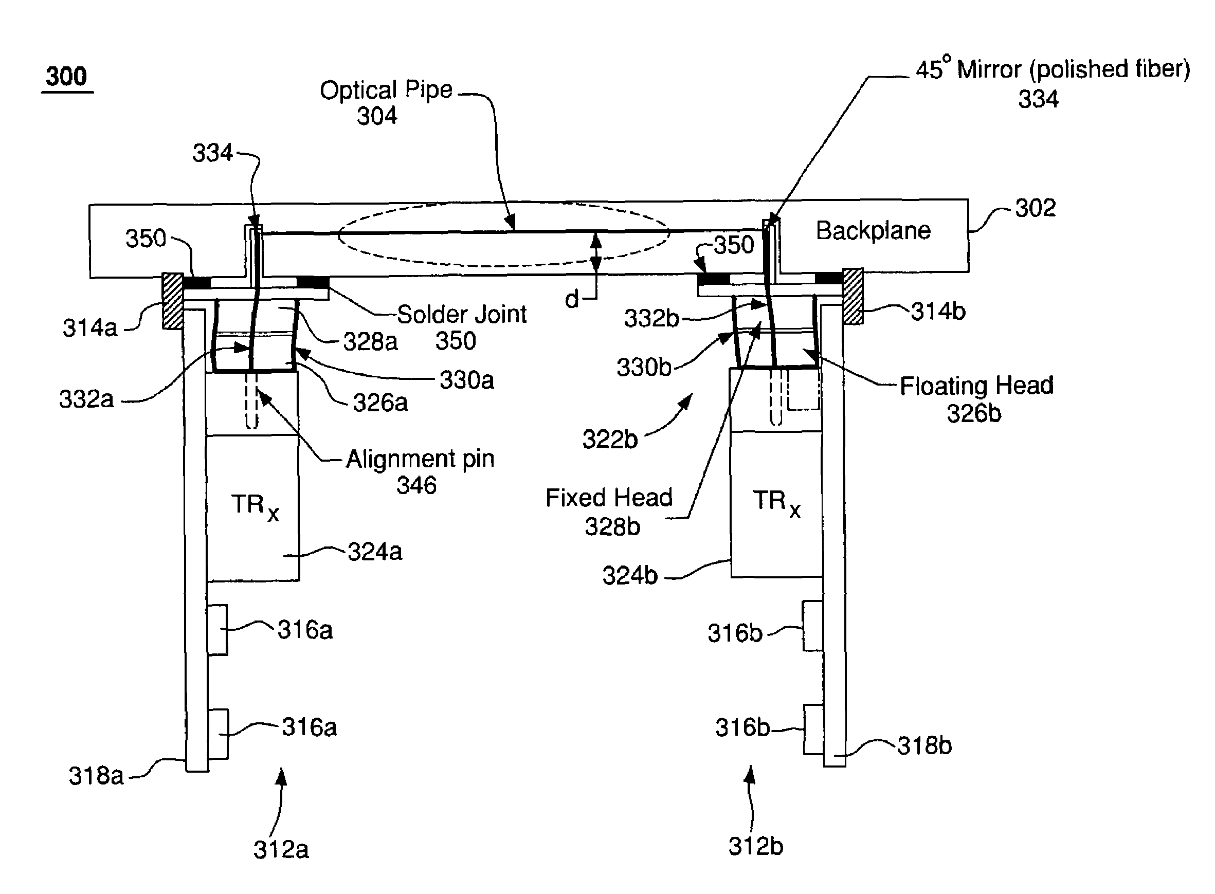
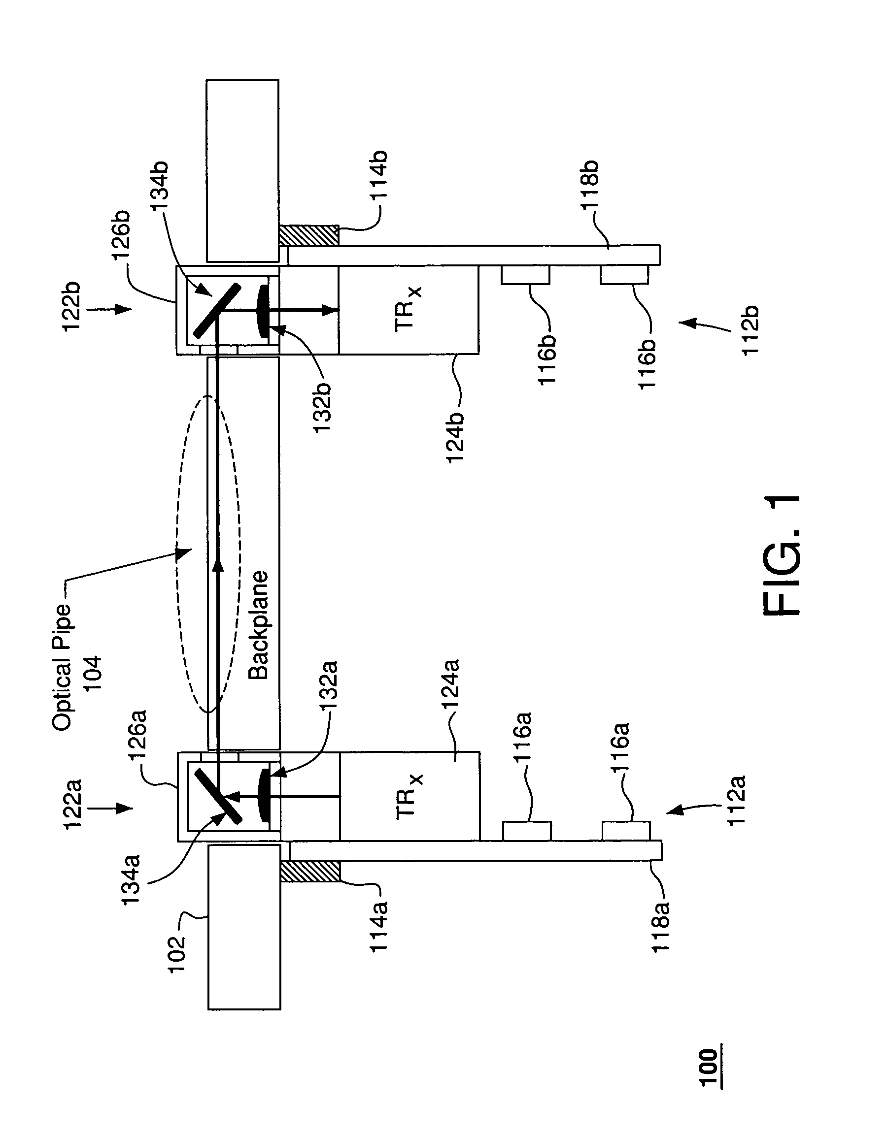
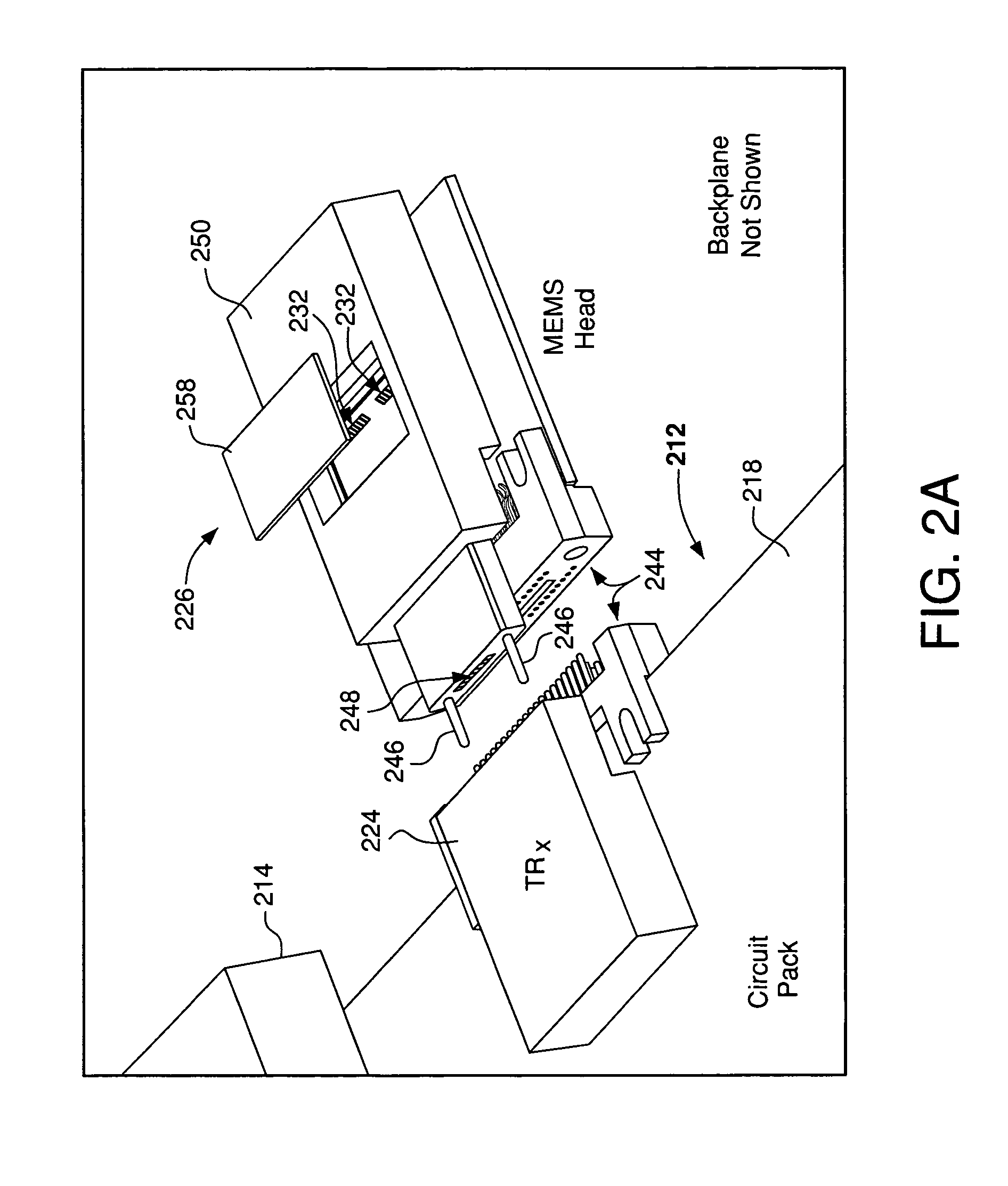
Coupler assembly for an optical backplane system
PatentInactiveUS7062132B2
Innovation
- A coupler assembly with movable optical elements, such as MEMS mirrors or flexible optical fibers, that can automatically adjust to maintain optical coupling by tracking changes in the relative position of the circuit pack and backplane, accommodating initial misalignment and subsequent deformations without operator intervention.

Signal path processing bias error detector
PatentActiveUS9698844B2
Innovation
- The method involves extracting and inverting a reference signal to compare it with the carrier signal after processing, allowing for the detection and compensation of signal-path processing errors by identifying and isolating the bias introduced by signal-processing components, which can be quickly reversed to isolate errors from sensor networks.


Manufacturing Standards for Optical Backplane Components
The manufacturing of optical backplane components requires adherence to stringent standards that directly impact signal integrity and path guide optimization. Current industry standards primarily follow IEC 61754 series for optical connectors and IPC-6012 for rigid printed circuit boards, though specific optical backplane standards remain fragmented across different organizations. The IEEE 802.3 Ethernet standards provide foundational requirements for optical transmission parameters, while ANSI/TIA-568 establishes performance criteria for optical fiber components.
Dimensional tolerances represent critical manufacturing parameters for optimized path guides. Connector alignment tolerances must maintain sub-micron precision, typically within ±0.5 micrometers for single-mode applications and ±2.5 micrometers for multimode systems. Waveguide positioning accuracy requires manufacturing tolerances of ±1 micrometer to prevent coupling losses that contribute to signal errors. Surface roughness specifications mandate Ra values below 0.1 micrometers for optical surfaces to minimize scattering losses.
Material standards encompass both substrate and optical components. Printed circuit board substrates must comply with flame retardancy requirements under UL 94 V-0 classification while maintaining low dielectric constants below 4.0 for high-frequency applications. Optical polymer materials require refractive index uniformity within ±0.001 across the component to ensure consistent light propagation. Glass transition temperatures must exceed 150°C to maintain dimensional stability during thermal cycling.
Quality control protocols mandate comprehensive testing procedures including insertion loss measurements, return loss verification, and crosstalk evaluation. Manufacturing facilities must implement statistical process control with Cpk values exceeding 1.33 for critical dimensions. Environmental testing standards require components to withstand temperature cycling from -40°C to +85°C with humidity exposure up to 95% relative humidity without performance degradation.
Emerging standards development focuses on establishing unified specifications for integrated optical backplanes. The Optical Internetworking Forum continues developing implementation agreements for optical backplane interfaces, while JEDEC works on thermal management standards specific to high-density optical interconnects. These evolving standards will provide clearer manufacturing guidelines for next-generation optical backplane systems with enhanced signal integrity performance.
Thermal Management Impact on Optical Signal Integrity
Thermal effects represent one of the most critical factors influencing optical signal integrity in backplane systems, where temperature variations can significantly degrade transmission quality and increase bit error rates. As optical components operate within confined backplane environments, heat generation from adjacent electronic components, power supplies, and high-density interconnects creates thermal gradients that directly impact the refractive index properties of optical materials and waveguide structures.
Temperature fluctuations cause dimensional changes in optical path guides through thermal expansion and contraction, leading to misalignment between optical fibers, connectors, and waveguide channels. These mechanical deformations alter the coupling efficiency between optical components, resulting in increased insertion losses and modal dispersion. Additionally, thermal stress can induce birefringence in optical materials, causing polarization-dependent losses that further compromise signal quality.
The refractive index temperature coefficient of optical materials becomes particularly problematic in backplane applications where temperature variations can exceed 40°C during normal operation. Silica-based waveguides exhibit a temperature coefficient of approximately 1×10^-5 per degree Celsius, which translates to significant wavelength shifts in dense wavelength division multiplexing systems. These shifts can cause channel crosstalk and reduce the effective bandwidth of optical interconnects.
Thermal cycling effects pose additional challenges for long-term reliability, as repeated expansion and contraction cycles can cause fatigue in optical adhesives, solder joints, and mechanical interfaces. This degradation progressively increases coupling losses and introduces intermittent signal interruptions that are difficult to predict and compensate for in real-time systems.
Advanced thermal management strategies have emerged to address these challenges, including the integration of micro-heat sinks, thermal interface materials with optimized thermal conductivity, and active cooling systems specifically designed for optical components. Temperature-compensated optical designs utilizing athermal waveguide materials and mechanically decoupled mounting systems have shown promising results in maintaining signal integrity across wide temperature ranges.
Real-time thermal monitoring and adaptive signal processing techniques are increasingly being implemented to dynamically compensate for temperature-induced signal degradation, enabling more robust optical backplane performance in demanding thermal environments.
Unlock deeper insights with PatSnap Eureka Quick Research — get a full tech report to explore trends and direct your research. Try now!
Generate Your Research Report Instantly with AI Agent
Supercharge your innovation with PatSnap Eureka AI Agent Platform!