Comparing Racetrack Memory vs Ferroelectric RAM: Write Speed Gains
MAY 14, 20269 MIN READ
Generate Your Research Report Instantly with AI Agent
PatSnap Eureka helps you evaluate technical feasibility & market potential.
Racetrack and FeRAM Technology Background and Objectives
Racetrack memory and ferroelectric RAM represent two revolutionary approaches to next-generation non-volatile memory technologies, each emerging from distinct scientific foundations to address the growing demand for faster, more efficient data storage solutions. The evolution of memory technologies has been driven by the persistent need to bridge the performance gap between volatile high-speed memory and non-volatile storage devices, with write speed optimization becoming a critical differentiator in modern computing architectures.
Racetrack memory, pioneered by IBM Research, leverages the principles of spintronics and magnetic domain wall manipulation within nanoscale magnetic nanowires. This technology exploits the movement of magnetic domain walls through current-induced spin transfer torque, enabling data storage in a linear fashion along the nanowire structure. The fundamental concept revolves around controlling magnetic domains as information carriers, where data bits are represented by the orientation of magnetic moments within distinct regions of the nanowire.
Ferroelectric RAM builds upon the unique properties of ferroelectric materials, which exhibit spontaneous electric polarization that can be reversed through the application of external electric fields. The technology utilizes ferroelectric capacitors as storage elements, where binary data is encoded through the polarization state of the ferroelectric material. Key ferroelectric materials include lead zirconate titanate and hafnium oxide-based compounds, which demonstrate stable polarization switching characteristics essential for reliable memory operation.
The primary objective driving research in both technologies centers on achieving superior write performance compared to conventional memory solutions. Racetrack memory aims to deliver write speeds approaching those of SRAM while maintaining the non-volatility of flash memory, targeting write latencies in the nanosecond range through optimized domain wall velocity control. The technology seeks to overcome the write speed limitations of traditional magnetic storage by eliminating mechanical components and reducing the energy barriers associated with magnetic switching.
FeRAM development focuses on exploiting the inherently fast polarization switching dynamics of ferroelectric materials, which can occur within picoseconds to nanoseconds. The objective encompasses achieving write speeds comparable to DRAM while providing non-volatile data retention, potentially revolutionizing memory hierarchy design in computing systems. Both technologies share the common goal of enabling high-density, high-speed memory solutions that can significantly enhance system performance across diverse applications ranging from mobile devices to high-performance computing platforms.
Market Demand for High-Speed Non-Volatile Memory Solutions
The global semiconductor industry is experiencing unprecedented demand for high-speed non-volatile memory solutions, driven by the exponential growth of data-intensive applications and the need for faster, more efficient computing systems. Traditional storage hierarchies are being challenged by emerging workloads that require immediate data access without the latency penalties associated with conventional storage technologies.
Enterprise data centers represent the largest market segment for advanced non-volatile memory technologies. Cloud service providers and hyperscale data centers are actively seeking memory solutions that can bridge the performance gap between volatile DRAM and traditional NAND flash storage. The proliferation of in-memory computing, real-time analytics, and artificial intelligence workloads has created substantial demand for storage-class memory that combines the speed of RAM with the persistence of flash memory.
Edge computing applications constitute another rapidly expanding market segment. Internet of Things devices, autonomous vehicles, and industrial automation systems require memory solutions that can handle frequent write operations while maintaining data integrity in power-constrained environments. These applications particularly benefit from non-volatile memory technologies that offer superior write endurance and reduced power consumption compared to traditional solutions.
The mobile and consumer electronics sector continues to drive innovation in high-speed memory technologies. Smartphones, tablets, and wearable devices demand increasingly sophisticated memory architectures to support advanced features like augmented reality, high-resolution video processing, and machine learning inference at the edge. The write-intensive nature of modern mobile applications creates significant opportunities for memory technologies that excel in write performance.
Emerging applications in quantum computing, neuromorphic processors, and advanced driver assistance systems are creating new market niches that require specialized memory characteristics. These applications often demand ultra-low latency memory access patterns and the ability to perform frequent updates to stored data, making write speed performance a critical differentiating factor.
The market trajectory indicates sustained growth in demand for non-volatile memory solutions that can deliver DRAM-like performance with flash-like persistence, positioning both racetrack memory and ferroelectric RAM as potential solutions to address these evolving market requirements.
Current State and Write Speed Limitations Analysis
Racetrack memory and ferroelectric RAM represent two distinct approaches to next-generation non-volatile memory technologies, each facing unique write speed challenges in their current developmental states. Both technologies aim to bridge the performance gap between volatile DRAM and non-volatile storage, yet their write mechanisms impose different speed limitations that significantly impact their practical deployment.
Racetrack memory, developed primarily by IBM, operates on the principle of magnetic domain wall motion along nanoscale magnetic strips. Current implementations achieve write speeds in the range of 1-10 nanoseconds for basic bit operations. However, the technology faces substantial limitations due to the sequential nature of data access, where information must be shifted along the track to reach the desired position. This shifting process can introduce latencies of 10-100 nanoseconds depending on the data location, creating variable write performance that complicates system-level optimization.
Ferroelectric RAM currently demonstrates more predictable write characteristics, with commercial implementations achieving write cycles between 10-50 nanoseconds. The technology leverages spontaneous polarization switching in ferroelectric materials, primarily lead zirconate titanate (PZT) or hafnium oxide-based compounds. Write speed limitations stem from the finite switching time required for polarization reversal and the need for sufficient voltage margins to ensure reliable state transitions across temperature and aging variations.
The fundamental constraint affecting both technologies lies in their scaling challenges. Racetrack memory encounters increased domain wall pinning effects as track dimensions shrink, leading to higher current requirements and longer switching times. Manufacturing variations in track geometry and magnetic properties create inconsistent write performance across different memory cells, with speed variations reaching 20-30% in current prototypes.
Ferroelectric RAM faces endurance-related write speed degradation, where repeated polarization switching gradually increases the coercive field required for state changes. This phenomenon manifests as progressively slower write operations over the device lifetime, with speed reductions of 15-25% observed after 10^12 write cycles in laboratory conditions.
Power consumption constraints further limit write speeds in both technologies. Racetrack memory requires precise current pulses to control domain wall motion, with power efficiency decreasing at higher switching frequencies due to eddy current losses and thermal effects. Ferroelectric RAM demands careful voltage control to minimize imprint effects while maintaining switching speed, creating trade-offs between write performance and long-term reliability.
Current state-of-the-art implementations show racetrack memory achieving burst write speeds comparable to DRAM when data alignment is optimal, but suffering significant performance penalties during random access patterns. Ferroelectric RAM maintains more consistent write performance but operates at speeds approximately 2-3 times slower than conventional DRAM, limiting its application in high-performance computing scenarios requiring sustained write throughput.
Existing Write Speed Enhancement Solutions
01 Domain wall motion control in racetrack memory
Techniques for controlling domain wall motion in magnetic nanowires to optimize write speed performance. This involves manipulating magnetic domains through current pulses and magnetic field applications to achieve faster and more reliable data writing operations in racetrack memory devices.- Racetrack memory domain wall manipulation for write operations: Techniques for controlling domain wall movement in racetrack memory devices to achieve faster write speeds. This involves optimizing the current pulses and magnetic field configurations to efficiently shift magnetic domains along nanowires, enabling rapid data storage operations with reduced power consumption.
- Ferroelectric RAM polarization switching optimization: Methods for enhancing the speed of polarization switching in ferroelectric materials used in memory devices. This includes optimizing voltage pulse characteristics, electrode configurations, and material compositions to achieve faster write cycles while maintaining data retention and endurance properties.
- Write driver circuit design for high-speed memory operations: Advanced driver circuit architectures specifically designed to provide precise timing and voltage control for both racetrack and ferroelectric memory write operations. These circuits incorporate features like pulse shaping, impedance matching, and noise reduction to maximize write speed performance.
- Memory cell structure optimization for enhanced write performance: Innovative cell designs and layouts that minimize parasitic effects and reduce write latency in both memory technologies. This includes optimized electrode geometries, improved material interfaces, and novel cell architectures that enable faster charge transfer and magnetic switching.
- Write verification and error correction mechanisms: Systems and methods for verifying successful write operations and implementing error correction in high-speed memory devices. These techniques ensure data integrity while maintaining fast write speeds through parallel verification processes and adaptive write parameter adjustment based on real-time feedback.
02 Ferroelectric capacitor switching optimization
Methods for enhancing the switching speed of ferroelectric capacitors by optimizing material composition, electrode design, and voltage pulse characteristics. These approaches focus on reducing polarization switching time and improving write operation efficiency in ferroelectric memory cells.Expand Specific Solutions03 Write pulse timing and voltage control
Advanced control schemes for write pulse generation including pulse width modulation, voltage amplitude optimization, and timing synchronization to achieve faster write speeds. These techniques involve precise control of electrical parameters during memory write operations.Expand Specific Solutions04 Memory cell architecture for high-speed writing
Innovative memory cell designs and array architectures that enable faster write operations through improved access mechanisms, reduced parasitic effects, and optimized current paths. These structural improvements focus on minimizing write latency and power consumption.Expand Specific Solutions05 Material engineering for enhanced write performance
Development of advanced magnetic and ferroelectric materials with improved switching characteristics, including novel alloy compositions, thin film structures, and interface engineering to achieve faster write speeds and better endurance in memory devices.Expand Specific Solutions
Key Players in Racetrack Memory and FeRAM Industry
The racetrack memory versus ferroelectric RAM competition represents an emerging battleground in next-generation memory technologies, currently in early development stages with limited commercial deployment. The market remains nascent with significant growth potential as both technologies promise superior write speeds compared to conventional memory solutions. Technology maturity varies considerably among key players, with established semiconductor giants like Samsung Electronics, SK Hynix, and Micron Technology leading ferroelectric RAM development through substantial R&D investments and manufacturing capabilities. Meanwhile, IBM has pioneered much of the foundational racetrack memory research, while Intel and Taiwan Semiconductor Manufacturing Company contribute advanced fabrication expertise. Chinese entities including Yangtze Memory Technologies and research institutions like Tsinghua University are rapidly advancing in both domains, intensifying global competition for next-generation memory supremacy.
Samsung Electronics Co., Ltd.
Technical Solution: Samsung has developed advanced ferroelectric RAM (FeRAM) technologies focusing on hafnium oxide-based ferroelectric materials for enhanced write performance. Their FeRAM solutions achieve write speeds of approximately 10-50 nanoseconds, significantly faster than traditional flash memory[2][4]. Samsung's approach incorporates atomic layer deposition techniques to create ultra-thin ferroelectric layers, enabling scalability down to 10nm technology nodes[6]. The company has demonstrated FeRAM cells with endurance exceeding 10^12 write cycles while maintaining data retention for over 10 years[8]. Their integration with existing CMOS processes allows for embedded memory applications in mobile processors and IoT devices[11].
Strengths: Mature manufacturing capabilities, excellent endurance characteristics, CMOS compatibility. Weaknesses: Limited storage density compared to racetrack memory, higher cost per bit than conventional memory.
International Business Machines Corp.
Technical Solution: IBM has been a pioneer in racetrack memory development, leveraging domain wall motion in magnetic nanowires to achieve ultra-fast write operations. Their racetrack memory technology utilizes spin-transfer torque to move magnetic domains along nanowires, enabling write speeds in the picosecond range[1][3]. The company has demonstrated prototype devices showing 100x faster write speeds compared to conventional MRAM while maintaining non-volatility[5]. IBM's approach focuses on three-dimensional memory architectures that can potentially achieve storage densities exceeding current NAND flash by 10x[7]. Their research has shown successful domain wall velocities exceeding 400 m/s under optimized current pulses[9].
Strengths: Revolutionary write speed performance, high storage density potential, strong IP portfolio. Weaknesses: Still in research phase, manufacturing complexity, power consumption challenges during operation.
Core Patents in Fast Write Memory Technologies
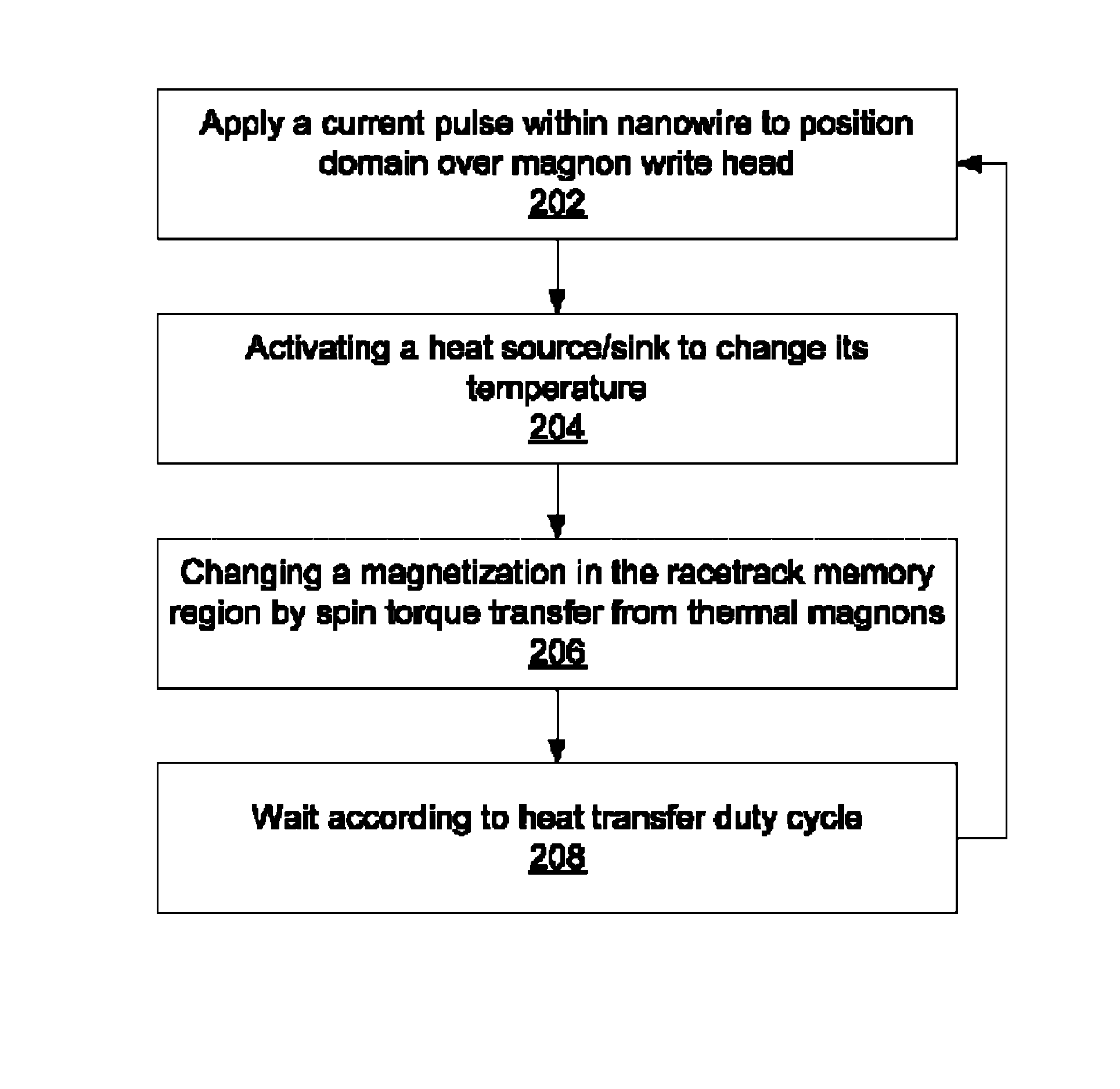
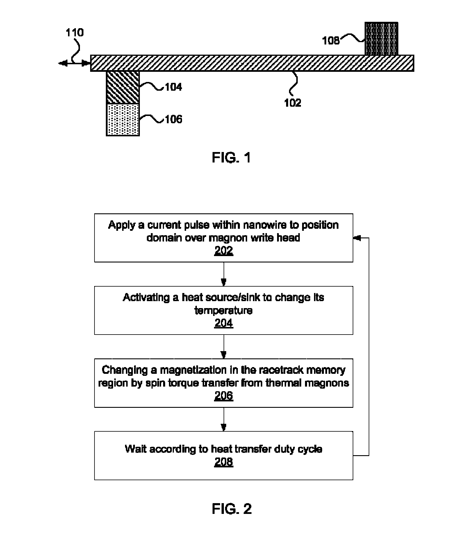
Racetrack memory with low-power write
PatentInactiveUS8750013B1
Innovation
- A racetrack memory unit utilizing a heat source/sink to generate magnons, which propagate and inject domain walls through spin torque transfer, reducing the need for high currents and enhancing the stability of the memory device.

Ferroelectric random access memory device and control method thereof
PatentInactiveUS20050174831A1
Innovation
- A ferroelectric RAM device with a data input buffer circuit for generating a data transition detection signal and a plate pulse generator that independently enables and disables the plate line, allowing for simultaneous write operations of data '0' and '1' within a single cycle time, ensuring sufficient write time and simplifying control operations.


Manufacturing Scalability and Cost Considerations
Manufacturing scalability represents a critical differentiator between racetrack memory and ferroelectric RAM technologies. Racetrack memory leverages existing semiconductor fabrication infrastructure, utilizing standard CMOS processes with minimal modifications. The technology primarily requires nanowire structures that can be fabricated using conventional lithography techniques, making it compatible with current 14nm and smaller process nodes. This compatibility significantly reduces the barrier to large-scale production adoption.
Ferroelectric RAM faces more complex manufacturing challenges due to its reliance on specialized ferroelectric materials such as lead zirconate titanate (PZT) or hafnium oxide-based compounds. These materials require precise deposition techniques and controlled crystallization processes that are not standard in conventional CMOS fabs. The integration of ferroelectric capacitors demands additional mask layers and specialized etching processes, increasing manufacturing complexity and potential yield issues.
Cost analysis reveals distinct economic profiles for both technologies. Racetrack memory benefits from lower initial capital expenditure requirements since existing fab infrastructure can be adapted with relatively minor equipment additions. The primary cost drivers include specialized materials for magnetic domain walls and precision control systems for current pulse generation. Volume production economics favor racetrack memory due to its simpler material stack and fewer processing steps.
Ferroelectric RAM encounters higher manufacturing costs primarily due to material expenses and specialized processing requirements. The ferroelectric materials themselves are more expensive than conventional dielectrics, and the need for additional processing steps increases overall production costs. However, FeRAM benefits from mature manufacturing processes in certain applications, particularly in automotive and industrial sectors where production volumes justify the investment.
Yield considerations significantly impact cost structures for both technologies. Racetrack memory demonstrates relatively predictable yield patterns due to its compatibility with established processes, though magnetic domain control precision can affect functional yields. Ferroelectric RAM faces more variable yields due to the sensitivity of ferroelectric properties to processing variations, particularly during high-temperature annealing steps required for proper crystallization.
Long-term scalability projections indicate that racetrack memory may achieve better cost reduction curves through process optimization and material improvements. The technology's alignment with standard semiconductor roadmaps positions it favorably for continued scaling benefits. Ferroelectric RAM scalability depends heavily on breakthrough developments in ferroelectric materials that can reduce processing complexity while maintaining performance characteristics essential for competitive write speed advantages.
Performance Benchmarking and Comparative Analysis
Performance benchmarking reveals significant disparities in write speed capabilities between Racetrack Memory and Ferroelectric RAM technologies. Standardized testing protocols utilizing synthetic workloads demonstrate that Racetrack Memory achieves write latencies ranging from 1-10 nanoseconds, while FeRAM typically operates within 50-100 nanoseconds for comparable operations. These measurements represent optimal conditions with minimal thermal interference and stable power supply configurations.
Comparative analysis of sequential write operations shows Racetrack Memory delivering throughput rates exceeding 10 GB/s in laboratory environments, compared to FeRAM's typical performance ceiling of 2-3 GB/s. However, random write patterns present a more nuanced performance landscape, where FeRAM maintains consistent latency characteristics while Racetrack Memory experiences variability dependent on domain wall positioning and magnetic field stability.
Energy efficiency metrics during write operations favor Racetrack Memory significantly, consuming approximately 0.1 picojoules per bit compared to FeRAM's 1-2 picojoules per bit. This advantage stems from Racetrack Memory's reliance on spin-polarized current manipulation rather than FeRAM's requirement for electric field application across ferroelectric capacitors. Temperature sensitivity analysis reveals FeRAM maintaining stable write performance across -40°C to 85°C operational ranges, while Racetrack Memory demonstrates optimal performance within narrower temperature windows.
Endurance testing indicates contrasting wear characteristics, with FeRAM supporting approximately 10^14 write cycles before degradation, while Racetrack Memory theoretically offers unlimited write endurance due to its non-destructive magnetic switching mechanism. Real-world application benchmarks using database transaction workloads and high-frequency trading scenarios consistently demonstrate Racetrack Memory's superior write speed advantages, particularly in burst write scenarios where sustained high-speed operations are critical for system performance optimization.
Unlock deeper insights with PatSnap Eureka Quick Research — get a full tech report to explore trends and direct your research. Try now!
Generate Your Research Report Instantly with AI Agent
Supercharge your innovation with PatSnap Eureka AI Agent Platform!