Dielectric Breakdown in High Frequency Applications
MAR 26, 20269 MIN READ
Generate Your Research Report Instantly with AI Agent
Patsnap Eureka helps you evaluate technical feasibility & market potential.
Dielectric Breakdown Background and HF Objectives
Dielectric breakdown represents a critical failure mechanism in electrical insulation systems where the dielectric material loses its insulating properties and becomes conductive under excessive electric field stress. This phenomenon occurs when the applied electric field exceeds the material's dielectric strength, leading to the formation of conductive channels and potentially catastrophic system failures. The breakdown process involves complex physical mechanisms including electron avalanche, thermal effects, and molecular degradation.
The evolution of dielectric breakdown research spans over a century, beginning with early investigations into gas discharge phenomena in the late 1800s. Initial studies focused on understanding breakdown in simple geometries and uniform fields. The mid-20th century brought significant advances in solid dielectric theory, with researchers developing models for intrinsic and extrinsic breakdown mechanisms. The introduction of polymer dielectrics in the 1950s expanded the field considerably, as these materials exhibited unique breakdown characteristics compared to traditional ceramics and glasses.
Modern dielectric breakdown research has been driven by the miniaturization of electronic devices and the increasing demand for high-performance insulation systems. The transition from low-frequency power applications to high-frequency electronics has fundamentally altered the breakdown landscape, introducing frequency-dependent effects that were previously negligible. Contemporary research encompasses multiscale modeling approaches, from quantum mechanical calculations of electron transport to macroscopic thermal and mechanical stress analysis.
High-frequency applications present unique challenges for dielectric materials due to several frequency-dependent phenomena. At elevated frequencies, dielectric losses increase significantly, leading to enhanced heating effects that can accelerate breakdown processes. The skin effect concentrates current density near conductor surfaces, creating localized high-field regions that are particularly susceptible to breakdown initiation. Additionally, high-frequency fields can excite molecular resonances and relaxation processes that alter the material's dielectric properties and breakdown strength.
The primary technical objectives in addressing high-frequency dielectric breakdown include developing predictive models that accurately capture frequency-dependent breakdown mechanisms, establishing reliable testing methodologies for high-frequency breakdown characterization, and identifying material design principles for enhanced high-frequency performance. Advanced objectives encompass the development of self-healing dielectric systems, integration of real-time breakdown monitoring capabilities, and the creation of adaptive insulation systems that can respond dynamically to changing operating conditions.
These objectives are driven by the critical need for reliable high-frequency electronic systems in applications ranging from 5G telecommunications infrastructure to electric vehicle power electronics, where dielectric failure can result in significant economic losses and safety hazards.
Market Demand for High Frequency Dielectric Solutions
The global demand for high-frequency dielectric solutions has experienced unprecedented growth driven by the rapid expansion of 5G networks, satellite communications, and advanced radar systems. Telecommunications infrastructure represents the largest market segment, where operators require dielectric materials capable of maintaining signal integrity at frequencies exceeding 28 GHz. The proliferation of millimeter-wave applications in automotive radar, wireless backhaul, and Internet of Things devices has created substantial market opportunities for specialized dielectric solutions.
Aerospace and defense sectors constitute another critical demand driver, particularly for applications involving phased array antennas, electronic warfare systems, and high-resolution imaging radar. These applications demand dielectric materials with exceptional thermal stability, low loss tangent, and resistance to breakdown under extreme operating conditions. The increasing deployment of satellite constellations for global broadband coverage has further amplified requirements for reliable high-frequency dielectric components.
Consumer electronics markets are witnessing growing demand for compact, high-performance dielectric solutions in smartphones, tablets, and wearable devices. The integration of multiple wireless communication standards within single devices necessitates dielectric materials that can operate efficiently across diverse frequency bands while maintaining miniaturized form factors. Gaming and virtual reality applications are emerging as significant demand generators, requiring low-latency, high-bandwidth connectivity solutions.
Industrial automation and smart manufacturing sectors are increasingly adopting wireless sensor networks and real-time monitoring systems operating at high frequencies. These applications require dielectric solutions that can withstand harsh industrial environments while maintaining consistent performance over extended operational periods. The automotive industry's transition toward autonomous vehicles has created substantial demand for reliable radar and communication systems operating in challenging electromagnetic environments.
Market growth is further supported by the expanding deployment of private 5G networks across various industries, including healthcare, logistics, and energy sectors. These specialized networks require customized dielectric solutions optimized for specific operational requirements and environmental conditions. The increasing emphasis on edge computing and distributed processing architectures has created additional demand for high-frequency interconnect solutions with superior dielectric properties.
Regional market dynamics reveal strong demand concentration in Asia-Pacific regions, driven by extensive telecommunications infrastructure development and consumer electronics manufacturing. North American and European markets demonstrate significant demand for aerospace, defense, and industrial applications, with emphasis on advanced material specifications and regulatory compliance requirements.
Current Dielectric Breakdown Challenges in HF Systems
High-frequency dielectric breakdown represents one of the most critical reliability challenges in modern electronic systems operating above 1 GHz. As frequencies increase, the electric field distribution within dielectric materials becomes increasingly non-uniform, creating localized stress concentrations that can initiate breakdown events at voltages significantly lower than DC predictions would suggest.
The primary challenge stems from the frequency-dependent nature of dielectric properties. At high frequencies, dielectric materials exhibit increased loss tangent values, leading to elevated internal heating and thermal runaway conditions. This phenomenon is particularly pronounced in polymer-based dielectrics commonly used in flexible circuits and high-density interconnects, where temperature coefficients can vary dramatically across the operational frequency spectrum.
Partial discharge activity emerges as another significant concern in HF applications. Unlike low-frequency systems where partial discharges follow predictable patterns, high-frequency environments generate complex discharge phenomena influenced by parasitic capacitances and inductances. These discharges create localized degradation zones that progressively weaken the dielectric structure, ultimately leading to catastrophic failure through treeing mechanisms.
Interface breakdown presents unique challenges in multilayer dielectric systems. High-frequency electric fields tend to concentrate at material interfaces due to permittivity mismatches, creating preferential breakdown paths. This issue is exacerbated in modern semiconductor packaging where multiple dielectric layers with varying properties must maintain isolation under rapidly switching voltage conditions.
Manufacturing-induced defects become increasingly problematic at high frequencies. Microscopic voids, contamination particles, and surface roughness that may be acceptable in low-frequency applications can serve as breakdown initiation sites when subjected to high-frequency electric fields. The skin effect further complicates this challenge by concentrating current density near conductor surfaces, intensifying local field strengths around defects.
Environmental factors compound these technical challenges significantly. Humidity absorption in hygroscopic dielectrics creates conductive pathways that dramatically reduce breakdown strength at high frequencies. Temperature cycling induces mechanical stress in dielectric materials, creating micro-cracks that propagate under high-frequency electric field stress, leading to premature failure in applications ranging from 5G infrastructure to automotive radar systems.
Existing HF Dielectric Breakdown Mitigation Solutions
01 High dielectric constant materials for breakdown resistance
Development of dielectric materials with high dielectric constants to improve breakdown voltage characteristics. These materials are designed to withstand higher electric field strengths before experiencing dielectric breakdown. The formulations focus on optimizing the molecular structure and composition to enhance the dielectric strength and reduce the likelihood of electrical failure under high voltage conditions.- High dielectric constant materials for breakdown resistance: Dielectric materials with high dielectric constants are developed to improve breakdown voltage resistance in electronic devices. These materials are designed to withstand higher electric field strengths before experiencing dielectric breakdown. The formulation focuses on optimizing the composition and structure of ceramic or polymer-based dielectrics to achieve enhanced electrical insulation properties and thermal stability under high voltage conditions.
- Composite dielectric materials with improved breakdown strength: Composite dielectric materials combining multiple components are formulated to enhance breakdown strength and reliability. These composites typically incorporate inorganic fillers into polymer matrices or layer different dielectric materials to create synergistic effects. The approach aims to reduce defects, improve uniformity, and increase the threshold voltage at which dielectric breakdown occurs through optimized interfacial properties and microstructure control.
- Thin film dielectric materials for miniaturized devices: Thin film dielectric materials are developed specifically for miniaturized electronic components where space constraints require reduced thickness without compromising breakdown performance. These materials utilize advanced deposition techniques and material engineering to maintain high breakdown field strength despite reduced dimensions. Special attention is given to surface quality, defect minimization, and interface engineering to prevent premature breakdown in thin film configurations.
- Self-healing dielectric materials for breakdown recovery: Self-healing dielectric materials are designed with the capability to recover from localized breakdown events, extending the operational lifetime of electrical systems. These materials incorporate mechanisms that can isolate or repair breakdown sites through chemical or physical processes. The technology focuses on preventing catastrophic failure by containing and neutralizing the effects of partial discharge or micro-breakdown events through innovative material compositions and architectures.
- Testing and characterization methods for dielectric breakdown: Advanced testing methodologies and characterization techniques are developed to evaluate dielectric breakdown behavior under various conditions. These methods include accelerated aging tests, partial discharge measurements, and breakdown voltage determination protocols. The approaches enable better prediction of material performance, identification of weak points in dielectric systems, and validation of material improvements through systematic evaluation of breakdown mechanisms and failure modes.
02 Composite dielectric materials with enhanced breakdown strength
Composite dielectric materials combining multiple components to achieve superior breakdown resistance. These materials typically incorporate fillers, polymers, or ceramic materials in specific ratios to create a synergistic effect that improves overall dielectric breakdown performance. The composite structure helps distribute electric field stress more uniformly and prevents localized breakdown.Expand Specific Solutions03 Thin film dielectric materials for microelectronic applications
Specialized thin film dielectric materials designed for microelectronic devices where breakdown prevention is critical. These materials are engineered at the nanoscale level to provide excellent insulation properties while maintaining minimal thickness. The focus is on achieving high breakdown field strength in compact configurations suitable for integrated circuits and semiconductor applications.Expand Specific Solutions04 Self-healing dielectric materials
Innovative dielectric materials with self-healing capabilities that can recover from partial breakdown events. These materials contain special additives or structural features that enable them to repair minor damage caused by electrical stress. The self-healing mechanism helps extend the operational lifetime and reliability of dielectric components by preventing catastrophic failure from localized breakdown sites.Expand Specific Solutions05 Testing and characterization methods for dielectric breakdown
Methods and apparatus for testing and characterizing dielectric breakdown properties of materials. These techniques involve applying controlled electrical stress to samples and measuring breakdown voltage, time-to-failure, and other relevant parameters. The testing protocols help evaluate material performance under various conditions and enable quality control in manufacturing processes.Expand Specific Solutions
Key Players in HF Dielectric and Insulation Industry
The dielectric breakdown in high frequency applications represents a mature yet rapidly evolving market segment driven by increasing demands for miniaturization and higher operating frequencies in electronic devices. The industry is experiencing significant growth, with market expansion fueled by 5G deployment, automotive electronics, and IoT applications. Technology maturity varies considerably across key players, with established Japanese companies like Murata Manufacturing, TDK Corp., Kyocera Corp., and Nichia Corp. leading in advanced ceramic and semiconductor solutions. European players such as Infineon Technologies and Siemens Energy contribute specialized power electronics expertise, while Asian manufacturers including Samsung Electronics, Taiwan Semiconductor Manufacturing, and Semiconductor Manufacturing International provide foundational semiconductor capabilities. Research institutions like Delft University of Technology and Industrial Technology Research Institute drive innovation in next-generation dielectric materials and breakdown mechanisms understanding, positioning the competitive landscape between established material science leaders and emerging high-frequency solution providers.
Murata Manufacturing Co. Ltd.
Technical Solution: Murata has developed advanced ceramic dielectric materials with enhanced breakdown voltage characteristics for high-frequency applications. Their multilayer ceramic capacitors (MLCCs) utilize proprietary dielectric formulations that maintain stable performance at frequencies up to several GHz while exhibiting breakdown voltages exceeding 1000V/μm. The company employs thin-film deposition techniques and precise control of grain boundaries to minimize defect density and improve dielectric strength. Their X7R and C0G dielectric materials demonstrate excellent temperature stability and low loss tangent properties, making them suitable for RF and microwave applications where dielectric breakdown resistance is critical.
Strengths: Industry-leading ceramic dielectric technology, excellent high-frequency performance. Weaknesses: Limited to ceramic-based solutions, higher cost compared to polymer alternatives.
TDK Corp.
Technical Solution: TDK has developed ferrite-based materials and multilayer components specifically designed to withstand high electric field stress in high-frequency environments. Their approach focuses on controlling the microstructure of ferrite materials through advanced sintering processes and dopant engineering to achieve breakdown voltages above 800V/μm at frequencies up to 10 GHz. The company's power inductors and transformers incorporate specialized insulation systems using polymer-ceramic composite materials that provide enhanced thermal conductivity and dielectric strength. TDK's proprietary material processing techniques enable precise control of porosity and grain size distribution, which are critical factors in preventing dielectric breakdown under high-frequency stress.
Strengths: Strong expertise in magnetic materials, comprehensive component portfolio. Weaknesses: Primarily focused on ferrite materials, limited polymer dielectric solutions.
Core Innovations in HF Dielectric Breakdown Prevention
Manufacturing and Use of Microperforated Substrates
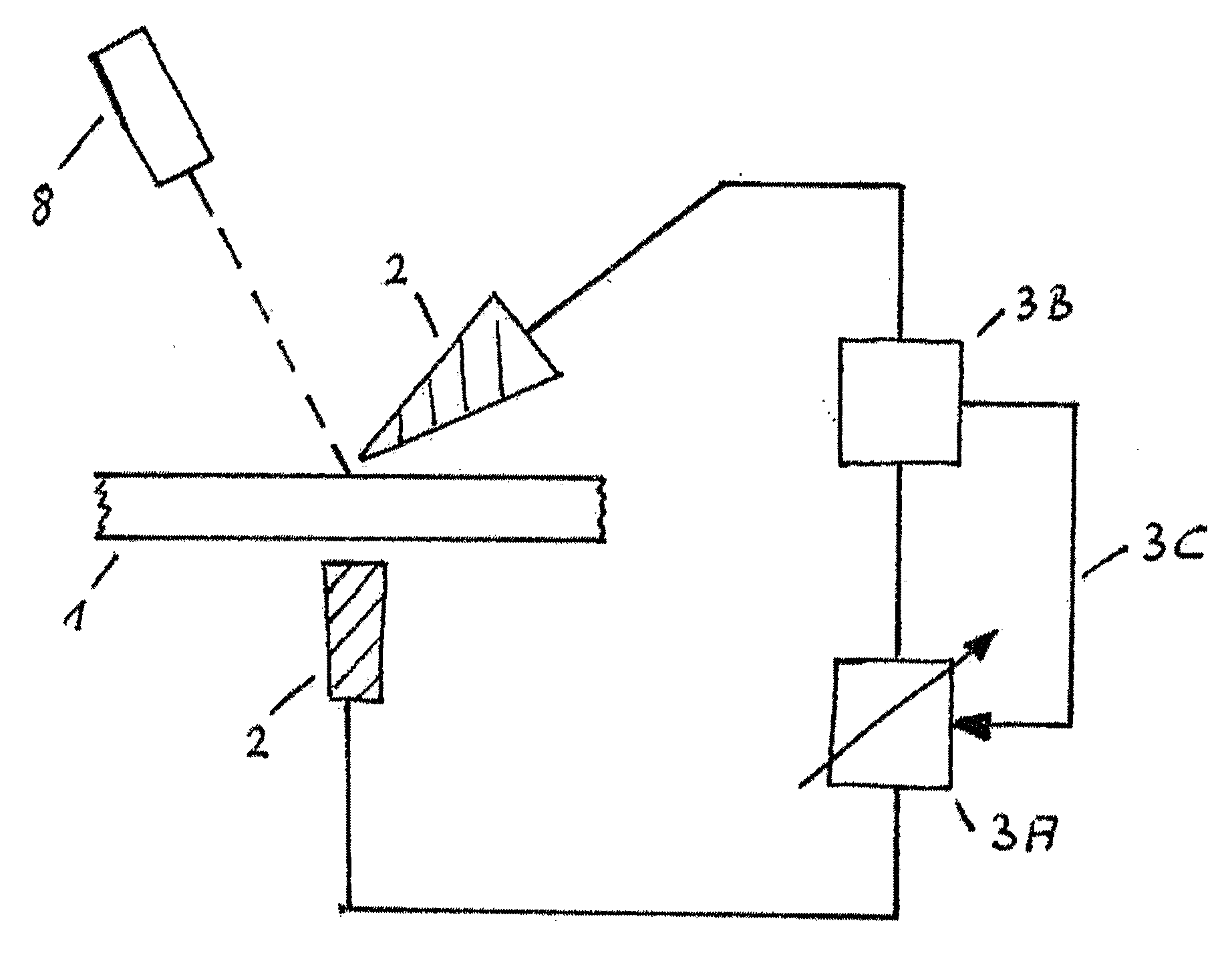
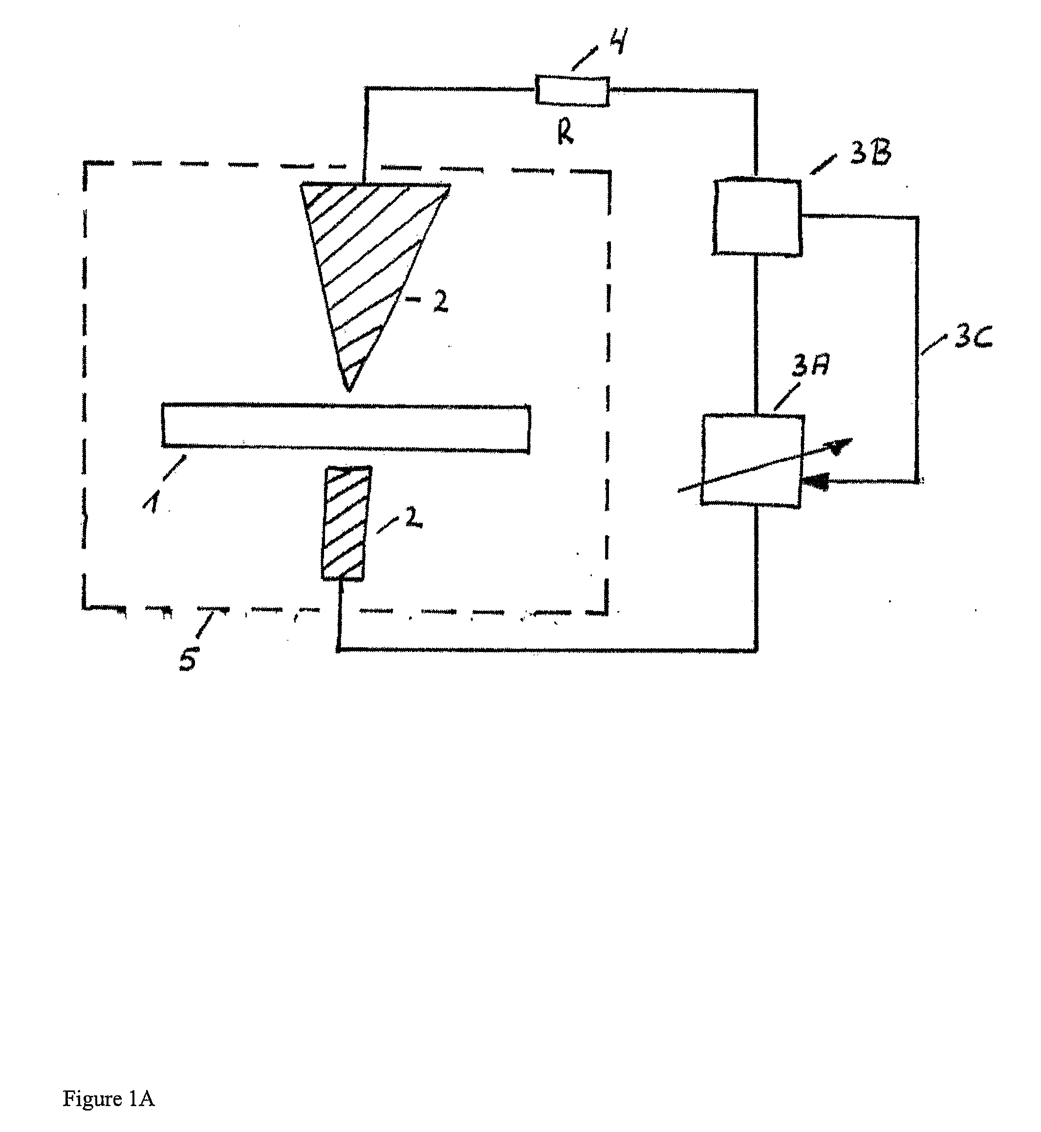
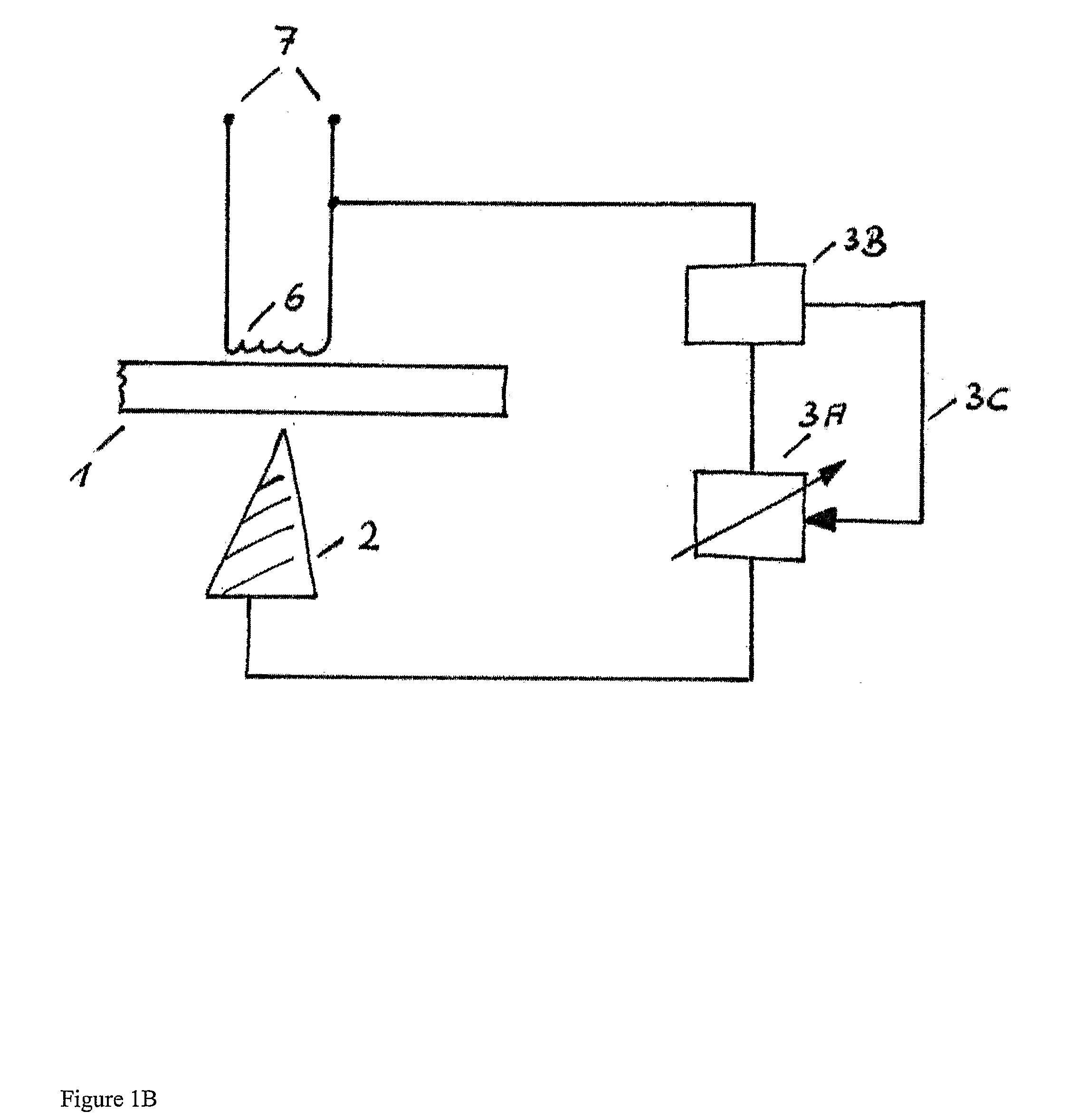
PatentActiveUS20080047935A1
Innovation
- A method involving controlled dielectric breakdown (CDEB) using a voltage supply and electronic feedback mechanisms to create precise holes in electrically insulating substrates, allowing for reproducible and cost-effective production of substrates with controlled hole diameters and aspect ratios.

Electrostatic discharge circuit and method of dissipating an electrostatic current
PatentInactiveUS20060175663A1
Innovation
- An electrostatic discharge circuit that alternately discharges ESD current through a bipolar transistor path and a resistor path, utilizing a switching pathway to form a low impedance discharge channel and then cut off current flow, preventing uncontrolled current increases by alternating between these paths.


Safety Standards for High Frequency Dielectric Systems
The establishment of comprehensive safety standards for high frequency dielectric systems has become increasingly critical as operating frequencies continue to escalate across various industrial applications. Current regulatory frameworks primarily encompass international standards such as IEC 60664 series for insulation coordination, IEEE 1584 for arc flash hazard calculations, and UL 840 for insulation coordination including clearance and creepage distances. These standards provide fundamental guidelines for dielectric system design, though many were originally developed for lower frequency applications and require continuous updates to address high frequency challenges.
International standardization bodies have recognized the urgent need for frequency-specific safety protocols. The International Electrotechnical Commission has initiated working groups to develop enhanced standards that specifically address dielectric breakdown phenomena at frequencies exceeding 1 MHz. These emerging standards focus on establishing minimum safety margins, testing methodologies, and failure prediction models tailored to high frequency environments where traditional safety factors may prove inadequate.
Testing and certification requirements for high frequency dielectric systems demand sophisticated measurement techniques and specialized equipment. Standard compliance testing now incorporates partial discharge measurements at operational frequencies, accelerated aging tests under high frequency stress conditions, and real-time monitoring of dielectric properties during operation. Certification bodies require comprehensive documentation of system behavior across the entire frequency spectrum, including harmonic analysis and electromagnetic compatibility assessments.
Regional variations in safety standards present significant challenges for global manufacturers. North American standards, governed by organizations such as NEMA and IEEE, often emphasize different safety margins compared to European IEC-based standards or Asian regional requirements. These discrepancies particularly affect high frequency applications where safety margins become more critical due to enhanced breakdown susceptibility.
The integration of predictive safety measures represents a paradigm shift in high frequency dielectric system standards. Modern safety protocols increasingly incorporate real-time monitoring systems, artificial intelligence-based failure prediction algorithms, and adaptive safety margins that adjust based on operational conditions. These advanced approaches enable proactive risk management rather than relying solely on static safety factors established during initial design phases.
Environmental Impact of HF Dielectric Materials
The environmental implications of high-frequency dielectric materials have become increasingly significant as electronic devices proliferate across consumer, industrial, and telecommunications sectors. Traditional dielectric materials used in high-frequency applications often contain substances that pose environmental challenges throughout their lifecycle, from manufacturing to disposal.
Perfluorinated compounds, commonly employed in high-performance dielectric applications due to their excellent electrical properties and thermal stability, present particular environmental concerns. These materials exhibit exceptional persistence in the environment and bioaccumulation potential, leading to regulatory scrutiny and phase-out initiatives in various jurisdictions. The manufacturing processes for these materials typically involve energy-intensive procedures and generate greenhouse gas emissions with high global warming potential.
Ceramic-based dielectric materials, while offering superior electrical performance at high frequencies, require high-temperature sintering processes that consume substantial energy and contribute to carbon emissions. The mining and processing of rare earth elements used in advanced ceramic formulations raise additional environmental concerns, including habitat disruption and water contamination risks.
Polymer-based dielectric materials present mixed environmental profiles. While some thermoplastic variants offer recyclability advantages, many high-performance polymers used in demanding applications are thermoset materials that resist conventional recycling methods. The incorporation of flame retardants and other additives further complicates end-of-life management and may introduce toxic substances into waste streams.
Emerging bio-based dielectric materials represent a promising avenue for reducing environmental impact. Research into cellulose-derived and other renewable feedstock materials has shown potential for maintaining adequate electrical performance while offering improved biodegradability and reduced carbon footprint during production.
The industry is increasingly adopting life cycle assessment methodologies to evaluate the comprehensive environmental impact of dielectric materials. This holistic approach considers raw material extraction, manufacturing energy consumption, transportation, use-phase efficiency, and end-of-life scenarios. Regulatory frameworks such as RoHS and REACH continue to drive material substitution efforts, pushing manufacturers toward more environmentally benign alternatives while maintaining the stringent performance requirements of high-frequency applications.
Unlock deeper insights with Patsnap Eureka Quick Research — get a full tech report to explore trends and direct your research. Try now!
Generate Your Research Report Instantly with AI Agent
Supercharge your innovation with Patsnap Eureka AI Agent Platform!