

Dielectric Breakdown vs Charge Accumulation
MAR 26, 20269 MIN READ
Generate Your Research Report Instantly with AI Agent
PatSnap Eureka helps you evaluate technical feasibility & market potential.
Dielectric Breakdown Background and Technical Objectives
Dielectric breakdown represents one of the most critical failure mechanisms in electrical insulation systems, fundamentally limiting the performance and reliability of electronic devices across multiple industries. This phenomenon occurs when an insulating material loses its dielectric properties under excessive electric field stress, leading to the formation of conductive pathways and potential catastrophic failure. The relationship between dielectric breakdown and charge accumulation has emerged as a pivotal research area, particularly as modern electronic systems demand higher power densities and miniaturization.
The historical development of dielectric breakdown theory traces back to the early 20th century when researchers first observed the correlation between electric field strength and insulation failure. Initial studies focused primarily on uniform field breakdown in simple geometries, but the understanding has evolved significantly with the recognition that charge accumulation plays a fundamental role in breakdown initiation and propagation. The advent of space charge measurement techniques in the 1980s revolutionized the field by enabling direct observation of charge distribution within dielectric materials.
Contemporary research has revealed that charge accumulation mechanisms significantly influence breakdown behavior through multiple pathways. Space charge formation creates local field enhancement, leading to non-uniform stress distribution that can trigger breakdown at field strengths well below theoretical limits. This understanding has shifted the focus from purely field-dependent models to comprehensive approaches that consider charge dynamics, material properties, and environmental factors.
The technical objectives in addressing dielectric breakdown versus charge accumulation encompass several critical dimensions. Primary goals include developing predictive models that accurately correlate charge accumulation patterns with breakdown probability, establishing measurement methodologies for real-time charge monitoring in operating systems, and creating material design strategies that minimize detrimental charge accumulation while maintaining desired dielectric properties.
Advanced characterization techniques now enable researchers to investigate the temporal and spatial evolution of charge accumulation under various stress conditions. These capabilities support the development of physics-based models that can predict breakdown behavior across different time scales, from microseconds in pulsed power applications to decades in high-voltage transmission systems. The integration of computational modeling with experimental validation has become essential for understanding the complex interplay between charge transport, trapping, and breakdown initiation.
The technological landscape continues to drive increasingly stringent requirements for dielectric performance, particularly in emerging applications such as electric vehicles, renewable energy systems, and high-frequency power electronics. These applications demand materials and designs that can withstand extreme operating conditions while maintaining long-term reliability, making the understanding of charge accumulation effects more critical than ever for ensuring system performance and safety.
The historical development of dielectric breakdown theory traces back to the early 20th century when researchers first observed the correlation between electric field strength and insulation failure. Initial studies focused primarily on uniform field breakdown in simple geometries, but the understanding has evolved significantly with the recognition that charge accumulation plays a fundamental role in breakdown initiation and propagation. The advent of space charge measurement techniques in the 1980s revolutionized the field by enabling direct observation of charge distribution within dielectric materials.
Contemporary research has revealed that charge accumulation mechanisms significantly influence breakdown behavior through multiple pathways. Space charge formation creates local field enhancement, leading to non-uniform stress distribution that can trigger breakdown at field strengths well below theoretical limits. This understanding has shifted the focus from purely field-dependent models to comprehensive approaches that consider charge dynamics, material properties, and environmental factors.
The technical objectives in addressing dielectric breakdown versus charge accumulation encompass several critical dimensions. Primary goals include developing predictive models that accurately correlate charge accumulation patterns with breakdown probability, establishing measurement methodologies for real-time charge monitoring in operating systems, and creating material design strategies that minimize detrimental charge accumulation while maintaining desired dielectric properties.
Advanced characterization techniques now enable researchers to investigate the temporal and spatial evolution of charge accumulation under various stress conditions. These capabilities support the development of physics-based models that can predict breakdown behavior across different time scales, from microseconds in pulsed power applications to decades in high-voltage transmission systems. The integration of computational modeling with experimental validation has become essential for understanding the complex interplay between charge transport, trapping, and breakdown initiation.
The technological landscape continues to drive increasingly stringent requirements for dielectric performance, particularly in emerging applications such as electric vehicles, renewable energy systems, and high-frequency power electronics. These applications demand materials and designs that can withstand extreme operating conditions while maintaining long-term reliability, making the understanding of charge accumulation effects more critical than ever for ensuring system performance and safety.
Market Demand for High-Voltage Dielectric Applications
The global high-voltage dielectric applications market is experiencing unprecedented growth driven by the critical need to address dielectric breakdown and charge accumulation challenges across multiple industrial sectors. Power transmission and distribution systems represent the largest demand segment, where utilities worldwide are upgrading aging infrastructure to handle increasing electrical loads while maintaining reliability and safety standards.
Electric vehicle manufacturers constitute a rapidly expanding market segment requiring advanced dielectric materials for battery systems, charging infrastructure, and power electronics. The automotive industry's transition toward electrification has intensified demand for dielectric solutions that can withstand high voltages while preventing charge accumulation that could lead to system failures or safety hazards.
Renewable energy installations, particularly wind turbines and solar power systems, generate substantial demand for high-performance dielectric materials. These applications require materials capable of operating reliably under varying environmental conditions while managing electrical stress and preventing breakdown phenomena that could compromise energy generation efficiency.
Industrial manufacturing sectors including aerospace, defense, and heavy machinery increasingly rely on high-voltage equipment requiring sophisticated dielectric solutions. These applications demand materials with superior breakdown strength and minimal charge accumulation characteristics to ensure operational safety and equipment longevity.
The semiconductor and electronics industries drive demand for specialized dielectric materials in power devices, capacitors, and insulation systems. As electronic devices operate at higher power densities and voltages, the need for materials that effectively manage dielectric stress and charge distribution becomes increasingly critical.
Emerging applications in energy storage systems, including grid-scale battery installations and capacitor banks, create new market opportunities for advanced dielectric technologies. These systems require materials capable of handling rapid charge-discharge cycles while maintaining structural integrity and preventing catastrophic breakdown events.
Market growth is further accelerated by stringent safety regulations and performance standards across industries, compelling manufacturers to adopt superior dielectric solutions that effectively address both breakdown prevention and charge accumulation management in high-voltage applications.
Electric vehicle manufacturers constitute a rapidly expanding market segment requiring advanced dielectric materials for battery systems, charging infrastructure, and power electronics. The automotive industry's transition toward electrification has intensified demand for dielectric solutions that can withstand high voltages while preventing charge accumulation that could lead to system failures or safety hazards.
Renewable energy installations, particularly wind turbines and solar power systems, generate substantial demand for high-performance dielectric materials. These applications require materials capable of operating reliably under varying environmental conditions while managing electrical stress and preventing breakdown phenomena that could compromise energy generation efficiency.
Industrial manufacturing sectors including aerospace, defense, and heavy machinery increasingly rely on high-voltage equipment requiring sophisticated dielectric solutions. These applications demand materials with superior breakdown strength and minimal charge accumulation characteristics to ensure operational safety and equipment longevity.
The semiconductor and electronics industries drive demand for specialized dielectric materials in power devices, capacitors, and insulation systems. As electronic devices operate at higher power densities and voltages, the need for materials that effectively manage dielectric stress and charge distribution becomes increasingly critical.
Emerging applications in energy storage systems, including grid-scale battery installations and capacitor banks, create new market opportunities for advanced dielectric technologies. These systems require materials capable of handling rapid charge-discharge cycles while maintaining structural integrity and preventing catastrophic breakdown events.
Market growth is further accelerated by stringent safety regulations and performance standards across industries, compelling manufacturers to adopt superior dielectric solutions that effectively address both breakdown prevention and charge accumulation management in high-voltage applications.
Current Dielectric Breakdown and Charge Accumulation Challenges
Dielectric breakdown and charge accumulation represent two of the most critical challenges in modern electrical insulation systems, fundamentally limiting the performance and reliability of high-voltage equipment across multiple industries. These phenomena are intrinsically linked yet present distinct technical obstacles that continue to constrain the development of next-generation electrical systems.
The primary challenge lies in understanding the complex relationship between electric field distribution and material degradation mechanisms. Current dielectric materials face significant limitations in their ability to withstand prolonged exposure to high electric fields without experiencing progressive deterioration. This degradation manifests through various pathways including partial discharge activity, space charge formation, and thermal aging, all of which contribute to eventual breakdown failure.
Space charge accumulation presents particularly complex challenges in modern insulation systems. The injection and trapping of charge carriers within dielectric materials create localized field enhancements that can exceed design thresholds, leading to premature failure. This phenomenon is especially problematic in DC applications where charge carriers have sufficient time to migrate and accumulate at material interfaces or defect sites.
Temperature-dependent behavior adds another layer of complexity to these challenges. Elevated operating temperatures accelerate charge carrier mobility while simultaneously reducing the activation energy required for breakdown initiation. This thermal sensitivity creates significant design constraints for equipment operating in harsh environments or under high load conditions.
Interface phenomena between different dielectric materials or between dielectrics and conductors represent critical failure points that remain poorly understood. These interfaces often exhibit different electrical properties compared to bulk materials, creating field concentration points and preferential breakdown paths that are difficult to predict and mitigate.
The challenge of measurement and characterization techniques further complicates progress in this field. Current diagnostic methods often lack the spatial and temporal resolution necessary to fully characterize charge accumulation patterns and pre-breakdown phenomena. This limitation hinders the development of accurate predictive models and effective mitigation strategies.
Manufacturing variability and material inhomogeneities introduce additional uncertainties that make it difficult to establish reliable design margins. Even minor variations in material composition, processing conditions, or geometric tolerances can significantly impact breakdown performance and charge accumulation behavior.
The primary challenge lies in understanding the complex relationship between electric field distribution and material degradation mechanisms. Current dielectric materials face significant limitations in their ability to withstand prolonged exposure to high electric fields without experiencing progressive deterioration. This degradation manifests through various pathways including partial discharge activity, space charge formation, and thermal aging, all of which contribute to eventual breakdown failure.
Space charge accumulation presents particularly complex challenges in modern insulation systems. The injection and trapping of charge carriers within dielectric materials create localized field enhancements that can exceed design thresholds, leading to premature failure. This phenomenon is especially problematic in DC applications where charge carriers have sufficient time to migrate and accumulate at material interfaces or defect sites.
Temperature-dependent behavior adds another layer of complexity to these challenges. Elevated operating temperatures accelerate charge carrier mobility while simultaneously reducing the activation energy required for breakdown initiation. This thermal sensitivity creates significant design constraints for equipment operating in harsh environments or under high load conditions.
Interface phenomena between different dielectric materials or between dielectrics and conductors represent critical failure points that remain poorly understood. These interfaces often exhibit different electrical properties compared to bulk materials, creating field concentration points and preferential breakdown paths that are difficult to predict and mitigate.
The challenge of measurement and characterization techniques further complicates progress in this field. Current diagnostic methods often lack the spatial and temporal resolution necessary to fully characterize charge accumulation patterns and pre-breakdown phenomena. This limitation hinders the development of accurate predictive models and effective mitigation strategies.
Manufacturing variability and material inhomogeneities introduce additional uncertainties that make it difficult to establish reliable design margins. Even minor variations in material composition, processing conditions, or geometric tolerances can significantly impact breakdown performance and charge accumulation behavior.
Existing Solutions for Dielectric Breakdown Prevention
01 Dielectric materials with enhanced breakdown voltage characteristics
Dielectric materials can be engineered to improve their breakdown voltage resistance through specific material compositions and structural modifications. These materials are designed to withstand higher electric field strengths before experiencing dielectric breakdown. The enhancement can be achieved through the use of composite materials, specific polymer formulations, or the incorporation of nanoparticles that improve the dielectric strength and reduce the likelihood of electrical failure under high voltage conditions.- Dielectric materials with enhanced breakdown voltage resistance: Dielectric materials can be engineered with specific compositions and structures to improve their resistance to electrical breakdown. This involves selecting materials with high dielectric strength and optimizing their molecular structure to withstand higher electric field intensities. Advanced polymer composites and ceramic materials are designed to prevent premature breakdown by controlling defects and impurities that could serve as breakdown initiation sites.
- Charge accumulation prevention through material modification: Charge accumulation in dielectric materials can be mitigated through various material modification techniques. These include incorporating conductive fillers, adjusting the material's conductivity, or using additives that facilitate charge dissipation. The modification helps to prevent localized charge buildup that can lead to dielectric breakdown and ensures more uniform electric field distribution within the material.
- Multi-layer dielectric structures for breakdown mitigation: Multi-layer dielectric configurations utilize alternating layers of different dielectric materials to enhance overall breakdown resistance. By strategically combining materials with varying dielectric constants and breakdown strengths, these structures can distribute electric stress more effectively and prevent charge accumulation at interfaces. The layered approach also provides redundancy, where if one layer begins to degrade, others can maintain insulation integrity.
- Surface treatment techniques for charge control: Surface treatment methods are employed to control charge accumulation on dielectric material surfaces. These techniques include plasma treatment, corona discharge treatment, and chemical modification of surface properties. Such treatments alter the surface energy and conductivity characteristics, enabling better charge dissipation and reducing the likelihood of surface flashover and breakdown events.
- Monitoring and detection systems for dielectric breakdown prediction: Advanced monitoring systems are developed to detect early signs of dielectric degradation and predict potential breakdown events. These systems utilize various sensing techniques to measure parameters such as partial discharge activity, temperature variations, and charge distribution patterns. By continuously monitoring these indicators, preventive measures can be implemented before catastrophic breakdown occurs, improving the reliability and lifespan of dielectric systems.
02 Charge accumulation prevention in dielectric layers
Methods and structures for preventing or reducing charge accumulation in dielectric materials involve the incorporation of charge dissipation layers or conductive pathways. These approaches help to distribute accumulated charges more evenly or provide controlled discharge paths to prevent localized charge buildup that can lead to dielectric breakdown. Techniques include the use of graded dielectric structures, intermediate conductive layers, or materials with controlled conductivity properties.Expand Specific Solutions03 Multi-layer dielectric structures for improved reliability
Multi-layer dielectric configurations are employed to enhance the overall dielectric performance and reduce breakdown susceptibility. These structures utilize alternating layers of different dielectric materials with varying properties to distribute electric field stress and minimize charge accumulation at interfaces. The layered approach provides redundancy and improved breakdown resistance compared to single-layer dielectric systems.Expand Specific Solutions04 Surface treatment and interface engineering for dielectric stability
Surface modification techniques and interface engineering are applied to dielectric materials to reduce charge trapping and improve breakdown characteristics. These methods involve surface passivation, interface layer formation, or chemical treatments that minimize defects and trap states at dielectric surfaces and interfaces. Such treatments help to reduce charge accumulation points and improve the long-term reliability of dielectric materials under electrical stress.Expand Specific Solutions05 Dielectric material testing and characterization methods
Advanced testing and characterization techniques are employed to evaluate dielectric breakdown behavior and charge accumulation properties. These methods include accelerated stress testing, charge injection measurements, and real-time monitoring of dielectric degradation. The characterization approaches help to predict dielectric lifetime, identify failure mechanisms, and optimize material selection for specific applications requiring high dielectric reliability.Expand Specific Solutions
Key Players in Dielectric Materials and High-Voltage Industry
The dielectric breakdown versus charge accumulation technology landscape represents a mature yet rapidly evolving sector within the broader semiconductor and energy storage industries. The market demonstrates significant scale, driven by applications spanning consumer electronics, automotive systems, and industrial equipment. Major established players including Samsung Electronics, Toshiba, Mitsubishi Electric, and Siemens leverage decades of research experience, while specialized companies like Capacitor Sciences and Space Charge LLC focus on breakthrough energy storage solutions. Technology maturity varies considerably across applications, with companies like Macronix, GLOBALFOUNDRIES, and Renesas advancing semiconductor-based solutions, while research institutions such as NASA and University of South Carolina contribute fundamental research. The competitive landscape shows consolidation among traditional electronics manufacturers alongside emerging specialized firms targeting next-generation dielectric materials and charge management systems.
Samsung Electronics Co., Ltd.
Technical Solution: Samsung has developed advanced dielectric materials and charge management techniques for their memory devices and displays. Their approach focuses on high-k dielectric materials with improved breakdown voltage characteristics while minimizing charge accumulation through engineered interface layers. The company utilizes atomic layer deposition (ALD) techniques to create ultra-thin, uniform dielectric films with controlled stoichiometry. Their technology incorporates charge trap engineering and interface optimization to reduce leakage currents and improve device reliability. Samsung's solutions are particularly effective in DRAM and flash memory applications where dielectric integrity is critical for data retention and device longevity.
Strengths: Industry-leading manufacturing capabilities, extensive R&D resources, proven track record in high-volume production. Weaknesses: Solutions may be optimized primarily for consumer electronics rather than specialized industrial applications.
Toshiba Corp.
Technical Solution: Toshiba has developed comprehensive solutions addressing dielectric breakdown through advanced material engineering and charge dissipation mechanisms. Their technology focuses on nanostructured dielectric materials with enhanced breakdown strength and controlled charge transport properties. The company employs multi-layer dielectric structures with graded compositions to distribute electric field stress and prevent localized breakdown. Their approach includes surface treatment techniques and dopant engineering to create controlled charge pathways that prevent accumulation while maintaining insulation properties. Toshiba's solutions are particularly effective in power electronics and high-voltage applications where reliable dielectric performance is essential.
Strengths: Strong expertise in power electronics, robust material science capabilities, established presence in industrial markets. Weaknesses: May face competition from specialized materials companies, limited focus on emerging applications.
Core Innovations in Charge Accumulation Control Technologies
Charge dissipative electrical interconnect
PatentInactiveUS20060022789A1
Innovation
- A charge-dissipative electrical interconnect comprising conductive elements, lossy dielectric layers, and grounding conductive elements that effectively dissipate electrical charge by transferring it to a zero volt reference, utilizing materials like thermoplastic polyester elastomers and silver-plated copper for enhanced charge mobility and mechanical robustness.


Method of making dielectric capacitors with increased dielectric breakdown strength
PatentActiveUS20130335882A1
Innovation
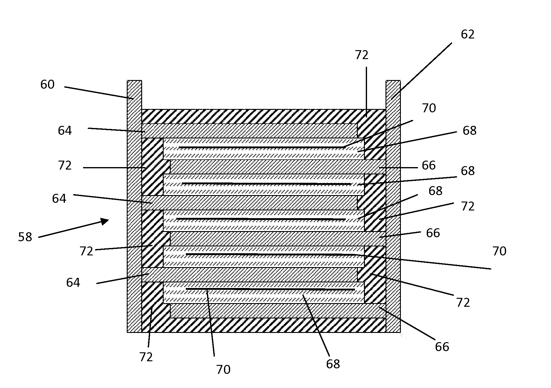
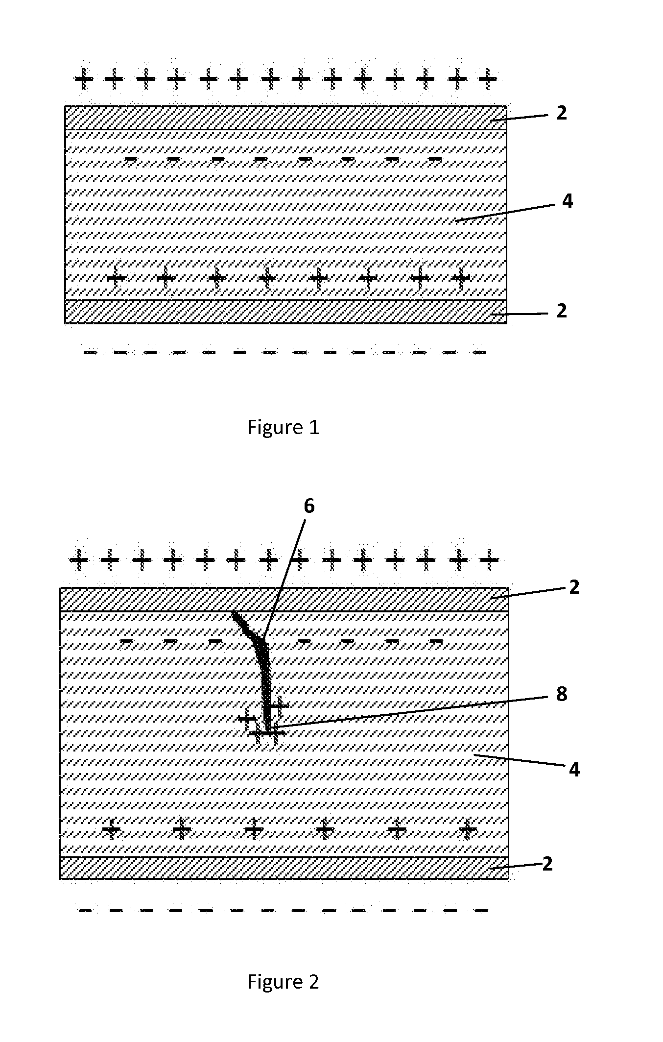
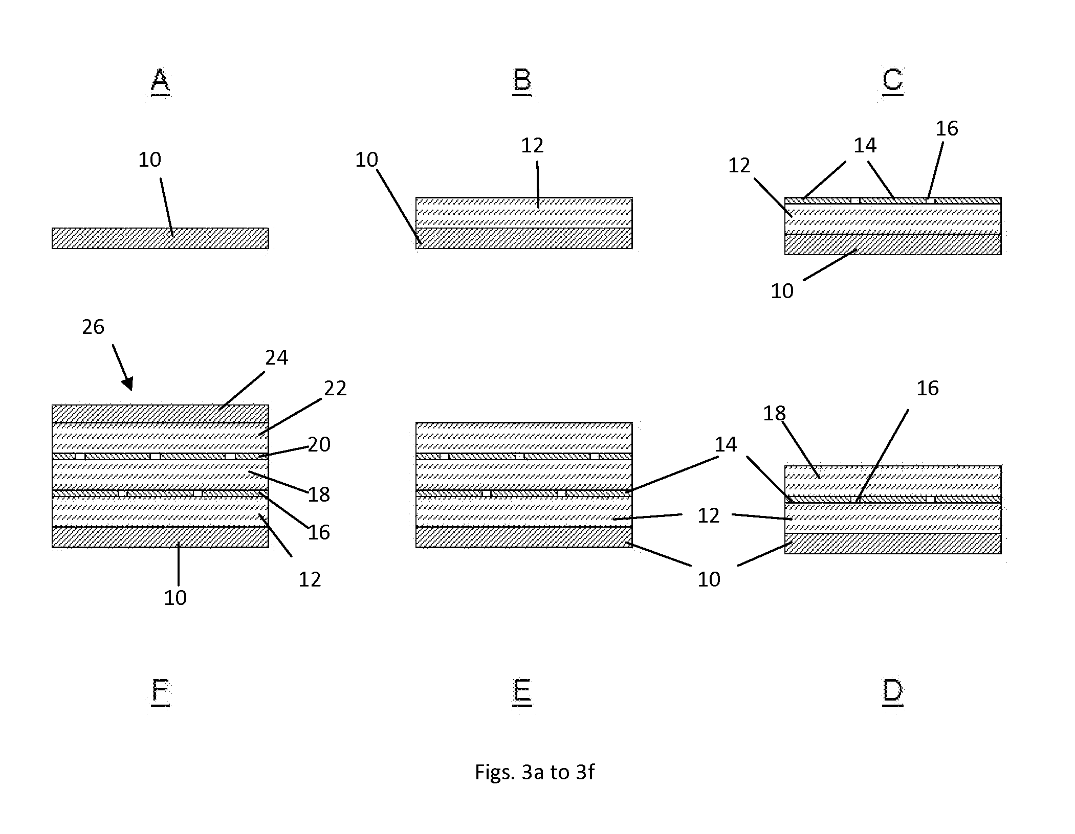
- Embedding thin conductive oxide layers within the ceramic dielectric material matrix to redistribute trapped charge and block the propagation of defects, thereby increasing dielectric breakdown strength and preventing rapid failure.

Safety Standards for High-Voltage Dielectric Systems
High-voltage dielectric systems require comprehensive safety standards to address the critical relationship between dielectric breakdown and charge accumulation phenomena. These standards establish fundamental protection protocols that ensure system reliability while preventing catastrophic failures that could result in equipment damage, personnel injury, or operational disruptions.
International safety standards, primarily governed by IEC 60071 series and IEEE standards, define specific testing methodologies and acceptance criteria for dielectric systems operating above 1kV. These frameworks establish minimum clearance distances, insulation coordination principles, and voltage withstand requirements that directly correlate with charge accumulation thresholds and breakdown voltage characteristics.
The standards mandate rigorous testing protocols including impulse voltage tests, power frequency withstand tests, and partial discharge measurements. These procedures specifically target the identification of charge accumulation patterns that precede dielectric breakdown events. Testing requirements typically specify voltage levels ranging from 1.5 to 3 times the rated operating voltage, with duration parameters designed to simulate long-term charge buildup scenarios.
Material qualification standards under IEC 60243 and ASTM D149 establish dielectric strength requirements that account for charge accumulation effects over extended operational periods. These specifications include aging tests, thermal cycling protocols, and humidity exposure assessments that evaluate how environmental factors influence charge distribution and breakdown susceptibility in dielectric materials.
Safety margins incorporated into these standards typically require breakdown voltages to exceed operational levels by factors of 2-5, depending on application criticality and environmental conditions. This approach ensures adequate protection against charge accumulation-induced failures while maintaining practical design constraints for commercial applications.
Compliance verification procedures mandate regular monitoring of partial discharge activity, insulation resistance measurements, and dielectric loss factor assessments. These monitoring protocols enable early detection of charge accumulation anomalies that could lead to premature breakdown events, supporting predictive maintenance strategies and operational safety assurance.
International safety standards, primarily governed by IEC 60071 series and IEEE standards, define specific testing methodologies and acceptance criteria for dielectric systems operating above 1kV. These frameworks establish minimum clearance distances, insulation coordination principles, and voltage withstand requirements that directly correlate with charge accumulation thresholds and breakdown voltage characteristics.
The standards mandate rigorous testing protocols including impulse voltage tests, power frequency withstand tests, and partial discharge measurements. These procedures specifically target the identification of charge accumulation patterns that precede dielectric breakdown events. Testing requirements typically specify voltage levels ranging from 1.5 to 3 times the rated operating voltage, with duration parameters designed to simulate long-term charge buildup scenarios.
Material qualification standards under IEC 60243 and ASTM D149 establish dielectric strength requirements that account for charge accumulation effects over extended operational periods. These specifications include aging tests, thermal cycling protocols, and humidity exposure assessments that evaluate how environmental factors influence charge distribution and breakdown susceptibility in dielectric materials.
Safety margins incorporated into these standards typically require breakdown voltages to exceed operational levels by factors of 2-5, depending on application criticality and environmental conditions. This approach ensures adequate protection against charge accumulation-induced failures while maintaining practical design constraints for commercial applications.
Compliance verification procedures mandate regular monitoring of partial discharge activity, insulation resistance measurements, and dielectric loss factor assessments. These monitoring protocols enable early detection of charge accumulation anomalies that could lead to premature breakdown events, supporting predictive maintenance strategies and operational safety assurance.
Environmental Impact of Dielectric Material Selection
The environmental implications of dielectric material selection have become increasingly critical as industries face mounting pressure to adopt sustainable practices while maintaining electrical performance standards. Traditional dielectric materials, particularly those containing halogenated compounds and heavy metals, pose significant environmental challenges throughout their lifecycle from manufacturing to disposal.
Manufacturing processes for conventional dielectric materials often involve energy-intensive procedures and generate substantial carbon emissions. Fluorinated polymers, while offering excellent dielectric properties, contribute to greenhouse gas emissions during production and exhibit extremely long atmospheric lifetimes. Similarly, ceramic dielectrics require high-temperature sintering processes that consume considerable energy and may release particulate matter into the atmosphere.
The disposal phase presents equally concerning environmental challenges. Many traditional dielectric materials are non-biodegradable and can persist in landfills for decades. When incinerated, certain materials release toxic compounds including dioxins and furans, contributing to air pollution and potential health hazards. Electronic waste containing these materials requires specialized handling and processing facilities, adding to disposal costs and environmental burden.
Emerging bio-based dielectric materials offer promising alternatives with reduced environmental footprints. Natural polymer-based dielectrics derived from cellulose, chitosan, and other renewable sources demonstrate comparable electrical properties while providing biodegradability. These materials can significantly reduce carbon emissions during production and eliminate long-term environmental persistence concerns.
Recycling initiatives for dielectric materials are gaining traction, though technical challenges remain. Advanced separation techniques enable recovery of valuable materials from electronic waste, reducing the demand for virgin raw materials. However, the complex composition of modern electronic devices often complicates efficient material recovery processes.
Life cycle assessment studies increasingly influence material selection decisions, considering environmental impact from raw material extraction through end-of-life management. Companies are developing comprehensive sustainability metrics that balance electrical performance requirements with environmental considerations, driving innovation toward more sustainable dielectric solutions while maintaining reliability standards for critical applications.
Manufacturing processes for conventional dielectric materials often involve energy-intensive procedures and generate substantial carbon emissions. Fluorinated polymers, while offering excellent dielectric properties, contribute to greenhouse gas emissions during production and exhibit extremely long atmospheric lifetimes. Similarly, ceramic dielectrics require high-temperature sintering processes that consume considerable energy and may release particulate matter into the atmosphere.
The disposal phase presents equally concerning environmental challenges. Many traditional dielectric materials are non-biodegradable and can persist in landfills for decades. When incinerated, certain materials release toxic compounds including dioxins and furans, contributing to air pollution and potential health hazards. Electronic waste containing these materials requires specialized handling and processing facilities, adding to disposal costs and environmental burden.
Emerging bio-based dielectric materials offer promising alternatives with reduced environmental footprints. Natural polymer-based dielectrics derived from cellulose, chitosan, and other renewable sources demonstrate comparable electrical properties while providing biodegradability. These materials can significantly reduce carbon emissions during production and eliminate long-term environmental persistence concerns.
Recycling initiatives for dielectric materials are gaining traction, though technical challenges remain. Advanced separation techniques enable recovery of valuable materials from electronic waste, reducing the demand for virgin raw materials. However, the complex composition of modern electronic devices often complicates efficient material recovery processes.
Life cycle assessment studies increasingly influence material selection decisions, considering environmental impact from raw material extraction through end-of-life management. Companies are developing comprehensive sustainability metrics that balance electrical performance requirements with environmental considerations, driving innovation toward more sustainable dielectric solutions while maintaining reliability standards for critical applications.
Unlock deeper insights with PatSnap Eureka Quick Research — get a full tech report to explore trends and direct your research. Try now!
Generate Your Research Report Instantly with AI Agent
Supercharge your innovation with PatSnap Eureka AI Agent Platform!