

Dielectric Breakdown vs Defects: Voids, Impurities, and Weak Points
MAR 26, 20269 MIN READ
Generate Your Research Report Instantly with AI Agent
PatSnap Eureka helps you evaluate technical feasibility & market potential.
Dielectric Breakdown Background and Technical Objectives
Dielectric breakdown represents one of the most critical failure mechanisms in electrical insulation systems, fundamentally limiting the performance and reliability of electronic devices across multiple industries. This phenomenon occurs when an insulating material loses its ability to resist electrical current flow under applied electric field stress, resulting in permanent damage and potential catastrophic failure of electronic components.
The historical development of dielectric breakdown understanding spans over a century, beginning with early observations in vacuum tubes and evolving through the semiconductor revolution to modern nanoscale devices. Initial theories focused on intrinsic breakdown mechanisms in perfect materials, but practical experience revealed that real-world failures predominantly occur due to material imperfections and manufacturing defects.
Contemporary electronic systems face unprecedented challenges as device miniaturization pushes electric field strengths to extreme levels. Modern semiconductor devices operate with gate oxide thicknesses measured in atomic layers, where even single atomic-scale defects can trigger breakdown events. This scaling trend has transformed dielectric breakdown from a bulk material property concern into a defect-dominated reliability issue.
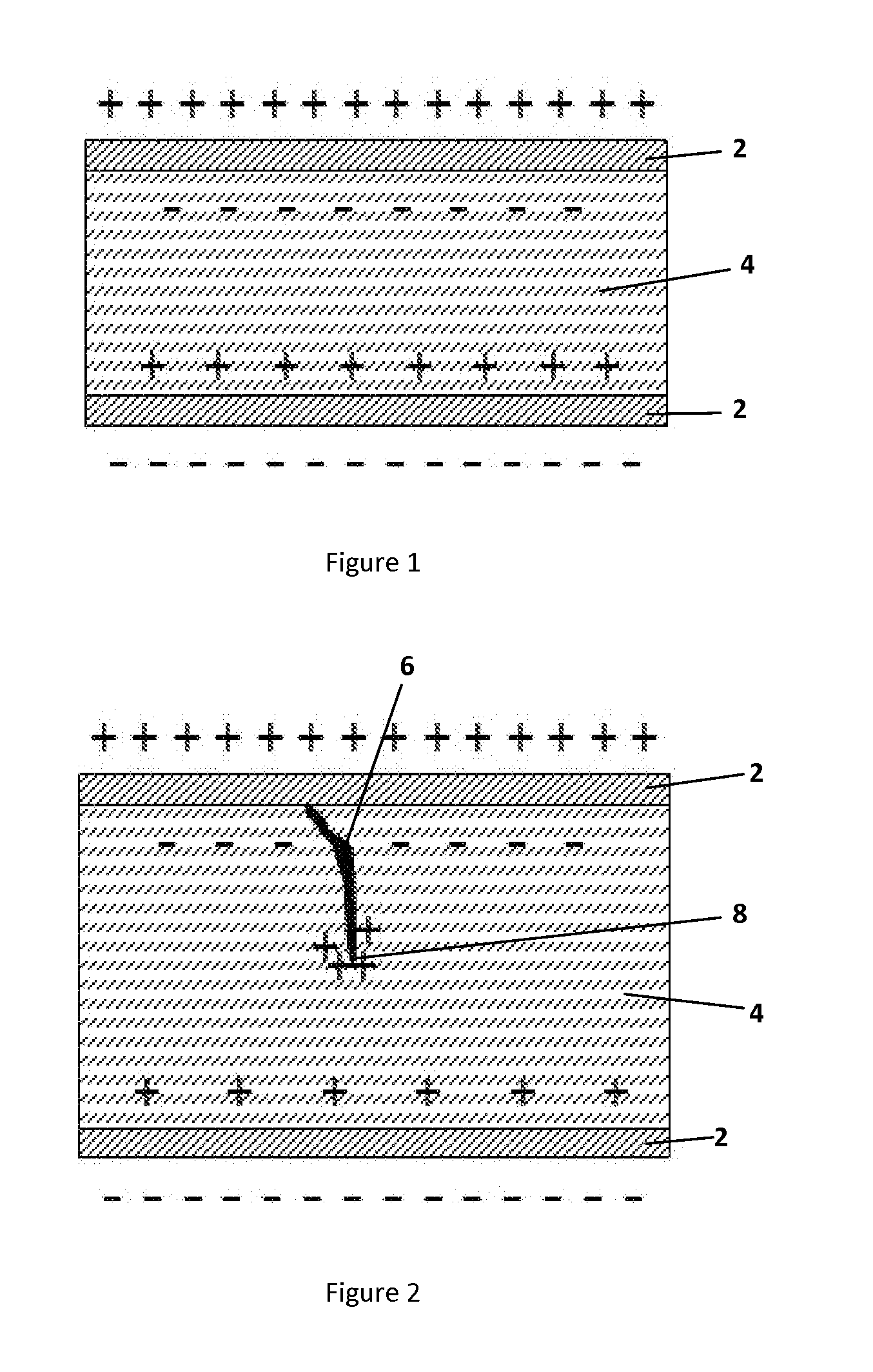
The relationship between material defects and breakdown susceptibility has emerged as a central research focus. Voids create localized field enhancement regions where breakdown preferentially initiates. Impurities introduce energy states within the bandgap, facilitating charge injection and transport processes that precede breakdown. Weak points, whether from processing variations or inherent material heterogeneity, serve as preferential breakdown sites under electrical stress.
Current technological objectives center on developing comprehensive understanding of defect-breakdown correlations to enable predictive reliability modeling. The primary goal involves establishing quantitative relationships between specific defect types, their spatial distribution, and breakdown probability distributions. This knowledge foundation supports the development of defect-tolerant design strategies and advanced screening methodologies.
Advanced characterization techniques now enable direct observation of breakdown precursor phenomena at nanoscale resolution. These capabilities support the development of physics-based models linking atomic-scale defect structures to macroscopic reliability metrics, representing a fundamental shift from empirical to predictive reliability engineering approaches in dielectric systems.
The historical development of dielectric breakdown understanding spans over a century, beginning with early observations in vacuum tubes and evolving through the semiconductor revolution to modern nanoscale devices. Initial theories focused on intrinsic breakdown mechanisms in perfect materials, but practical experience revealed that real-world failures predominantly occur due to material imperfections and manufacturing defects.
Contemporary electronic systems face unprecedented challenges as device miniaturization pushes electric field strengths to extreme levels. Modern semiconductor devices operate with gate oxide thicknesses measured in atomic layers, where even single atomic-scale defects can trigger breakdown events. This scaling trend has transformed dielectric breakdown from a bulk material property concern into a defect-dominated reliability issue.
The relationship between material defects and breakdown susceptibility has emerged as a central research focus. Voids create localized field enhancement regions where breakdown preferentially initiates. Impurities introduce energy states within the bandgap, facilitating charge injection and transport processes that precede breakdown. Weak points, whether from processing variations or inherent material heterogeneity, serve as preferential breakdown sites under electrical stress.
Current technological objectives center on developing comprehensive understanding of defect-breakdown correlations to enable predictive reliability modeling. The primary goal involves establishing quantitative relationships between specific defect types, their spatial distribution, and breakdown probability distributions. This knowledge foundation supports the development of defect-tolerant design strategies and advanced screening methodologies.
Advanced characterization techniques now enable direct observation of breakdown precursor phenomena at nanoscale resolution. These capabilities support the development of physics-based models linking atomic-scale defect structures to macroscopic reliability metrics, representing a fundamental shift from empirical to predictive reliability engineering approaches in dielectric systems.
Market Demand for Reliable Dielectric Materials
The global electronics industry faces unprecedented challenges in ensuring dielectric material reliability as device miniaturization and performance demands continue to escalate. Modern electronic systems require dielectric materials that can withstand increasingly high electric field strengths while maintaining structural integrity over extended operational periods. The proliferation of electric vehicles, renewable energy systems, and high-frequency communication devices has intensified the need for materials that demonstrate exceptional resistance to breakdown phenomena caused by manufacturing defects.
Semiconductor manufacturers and electronic component producers are experiencing mounting pressure to deliver products with enhanced reliability metrics. The automotive electronics sector, particularly in electric and hybrid vehicles, demands dielectric materials capable of operating under extreme conditions without failure. Power electronics applications in industrial automation and grid infrastructure require materials that can handle high voltage operations while minimizing the risk of catastrophic breakdown events.
The telecommunications industry's transition to higher frequency bands and increased power densities has created substantial market opportunities for advanced dielectric materials. Data center operators and cloud service providers are seeking materials that can support high-performance computing applications while maintaining thermal stability and electrical integrity. The growing Internet of Things ecosystem further amplifies the demand for reliable dielectric solutions across diverse application environments.
Market drivers include stringent regulatory requirements for safety and reliability in critical applications, particularly in aerospace, medical devices, and energy storage systems. The increasing cost of product recalls and warranty claims has motivated manufacturers to invest in superior dielectric materials that minimize defect-related failures. Quality assurance standards continue to evolve, requiring materials that can demonstrate consistent performance despite the presence of microscopic voids, impurities, and other structural weaknesses.
The renewable energy sector presents significant growth opportunities, as solar inverters, wind turbine electronics, and energy storage systems require dielectric materials with exceptional longevity and reliability. Battery management systems and charging infrastructure demand materials that can withstand repeated thermal cycling and electrical stress without degradation.
Emerging applications in quantum computing, advanced sensors, and next-generation display technologies are creating niche markets for specialized dielectric materials with unprecedented purity and structural uniformity requirements. These applications often require custom material formulations that address specific defect-related challenges while maintaining compatibility with existing manufacturing processes.
Current State of Dielectric Defect Analysis
The current landscape of dielectric defect analysis has evolved significantly with the advancement of characterization techniques and computational modeling capabilities. Traditional methods such as scanning electron microscopy (SEM) and transmission electron microscopy (TEM) remain fundamental for identifying structural defects including voids, grain boundaries, and interfacial irregularities. These techniques provide high-resolution imaging that enables direct visualization of defect morphology and distribution patterns within dielectric materials.
Advanced spectroscopic methods have emerged as powerful tools for chemical defect identification. X-ray photoelectron spectroscopy (XPS) and secondary ion mass spectrometry (SIMS) enable precise detection of impurity concentrations and chemical composition variations that contribute to localized electric field enhancement. Energy-dispersive X-ray spectroscopy (EDS) mapping provides spatial distribution analysis of elemental impurities, revealing correlation patterns between chemical heterogeneity and breakdown susceptibility.
Electrical characterization techniques have become increasingly sophisticated in correlating defect presence with breakdown behavior. Current-voltage (I-V) measurements under controlled stress conditions reveal leakage pathways associated with specific defect types. Time-dependent dielectric breakdown (TDDB) testing protocols have been standardized to assess reliability metrics while identifying failure mechanisms linked to particular defect categories.
Computational approaches now complement experimental methods through density functional theory (DT) calculations and molecular dynamics simulations. These theoretical frameworks predict defect formation energies, electronic states, and charge transport properties, providing mechanistic insights into how specific defects influence breakdown initiation and propagation.
Machine learning algorithms are increasingly integrated into defect analysis workflows, enabling pattern recognition in large datasets from multiple characterization techniques. These approaches facilitate automated defect classification and correlation analysis between defect parameters and breakdown statistics.
Despite these advances, significant challenges persist in establishing quantitative relationships between defect characteristics and breakdown probability. The multi-scale nature of breakdown phenomena, spanning from atomic-level defects to device-level failure, requires integrated analysis approaches that current methodologies struggle to address comprehensively.
Existing Defect Detection and Prevention Solutions
01 High dielectric constant materials for breakdown resistance
Dielectric materials with high dielectric constants are developed to improve breakdown voltage resistance in electronic devices. These materials are engineered to withstand higher electric field strengths before experiencing dielectric breakdown. The formulation focuses on optimizing the molecular structure and composition to enhance the dielectric strength while maintaining stable electrical properties across various operating conditions.- High dielectric constant materials for breakdown resistance: Dielectric materials with high dielectric constants are developed to improve breakdown voltage resistance in electronic devices. These materials are engineered to withstand higher electric field strengths before experiencing dielectric breakdown. The formulation focuses on optimizing the molecular structure and composition to enhance the dielectric strength while maintaining stable electrical properties across various operating conditions.
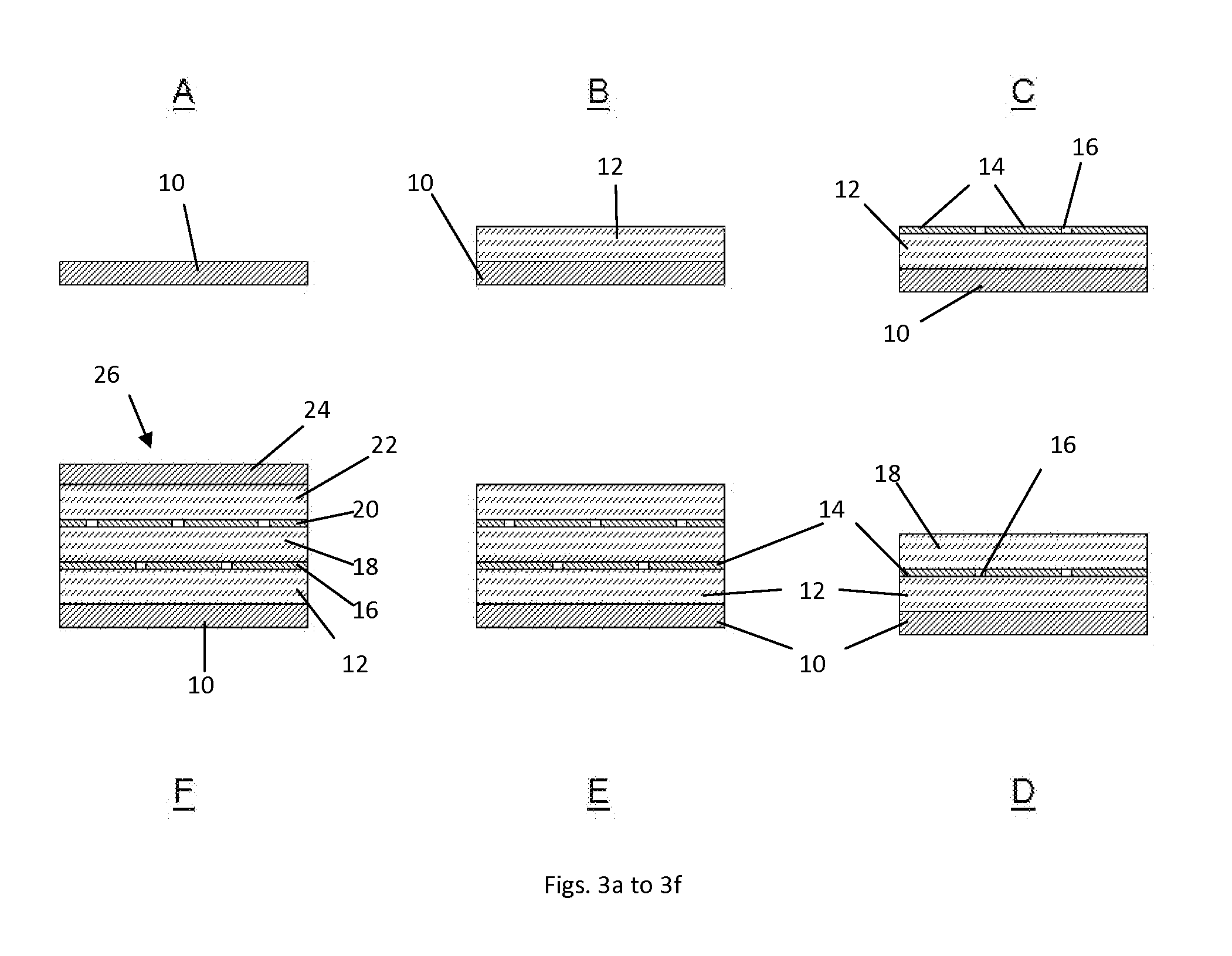
- Composite dielectric materials with enhanced breakdown strength: Composite dielectric materials combine multiple components to achieve superior breakdown resistance compared to single-phase materials. These composites typically incorporate inorganic fillers or nanoparticles dispersed within a polymer matrix to create interfaces that impede electrical breakdown pathways. The synergistic effect of different materials results in improved dielectric breakdown voltage and thermal stability.
- Thin film dielectric layers for semiconductor applications: Thin film dielectric materials are specifically designed for semiconductor and microelectronic applications where precise control of breakdown characteristics is critical. These films are deposited using advanced techniques to achieve uniform thickness and minimal defects. The materials are optimized to prevent breakdown at reduced dimensions while maintaining low leakage current and high reliability in integrated circuits.
- Self-healing dielectric materials: Self-healing dielectric materials incorporate mechanisms that allow the material to recover from localized breakdown events. These materials contain additives or structural features that can isolate or repair breakdown channels, preventing catastrophic failure. The self-healing capability extends the operational lifetime of capacitors and other dielectric components by mitigating the effects of partial discharge and micro-breakdown events.
- Testing and characterization methods for dielectric breakdown: Advanced testing methodologies are employed to evaluate and predict dielectric breakdown behavior under various stress conditions. These methods include accelerated aging tests, partial discharge measurements, and high-voltage stress testing to determine breakdown voltage thresholds. Characterization techniques help in understanding failure mechanisms and improving material design for enhanced breakdown resistance in practical applications.
02 Composite dielectric materials with enhanced breakdown strength
Composite dielectric materials combine multiple components to achieve superior breakdown resistance. These formulations typically incorporate inorganic fillers, polymers, or ceramic materials to create a synergistic effect that increases the overall dielectric breakdown threshold. The composite approach allows for tailoring of electrical properties while improving mechanical strength and thermal stability of the dielectric layer.Expand Specific Solutions03 Thin film dielectric materials for miniaturized devices
Thin film dielectric materials are specifically designed for applications requiring compact dimensions without compromising breakdown voltage performance. These materials utilize advanced deposition techniques and material engineering to create ultra-thin layers with high dielectric strength. The formulations address challenges related to defect minimization and uniform thickness distribution to prevent localized breakdown events.Expand Specific Solutions04 Self-healing dielectric materials for breakdown recovery
Self-healing dielectric materials incorporate mechanisms that allow the material to recover from minor breakdown events. These formulations include additives or structural features that can isolate or repair breakdown channels, extending the operational lifetime of the dielectric component. The technology focuses on preventing catastrophic failure by containing and neutralizing localized breakdown sites.Expand Specific Solutions05 Temperature-stable dielectric materials for harsh environments
Temperature-stable dielectric materials are formulated to maintain consistent breakdown voltage characteristics across wide temperature ranges. These materials incorporate thermally stable polymers, ceramics, or hybrid compositions that resist degradation under thermal stress. The formulations address thermal expansion mismatch and chemical stability to ensure reliable performance in demanding environmental conditions.Expand Specific Solutions
Key Players in Dielectric Materials Industry
The dielectric breakdown versus defects technology landscape represents a mature yet rapidly evolving sector driven by increasing demands for higher performance electronic components and energy storage systems. The market spans multiple billion-dollar segments including semiconductors, capacitors, and advanced materials, with established players like Intel, Taiwan Semiconductor Manufacturing, Applied Materials, and Texas Instruments leading semiconductor applications, while Samsung Electro-Mechanics, Murata Manufacturing, and TDK Electronics dominate the passive components space. Technology maturity varies significantly across applications - traditional semiconductor dielectric technologies are well-established, whereas emerging areas like high-energy-density capacitors (Capacitor Sciences) and advanced packaging solutions remain in development phases. The competitive landscape shows strong geographic distribution with Asian manufacturers (Samsung, Murata, TSMC) competing alongside American (Intel, Applied Materials, Micron) and European players (TDK Electronics), indicating a globally distributed but technologically concentrated market where defect mitigation and breakdown prevention drive continuous innovation.
Applied Materials, Inc.
Technical Solution: Applied Materials develops advanced process control and metrology solutions for dielectric breakdown analysis, utilizing plasma-enhanced chemical vapor deposition (PECVD) and atomic layer deposition (ALD) technologies to minimize void formation and impurities in dielectric films. Their Reflexion LK Prime system enables real-time monitoring of film quality during deposition, detecting potential weak points through advanced optical and electrical characterization. The company's integrated approach combines materials engineering with in-situ process monitoring to achieve dielectric breakdown voltages exceeding 10 MV/cm while maintaining film uniformity across 300mm wafers.
Strengths: Industry-leading process control technology, comprehensive materials characterization capabilities. Weaknesses: High equipment costs, complex integration requirements for existing fabs.
Samsung Electro-Mechanics Co., Ltd.
Technical Solution: Samsung Electro-Mechanics develops advanced dielectric materials and processing technologies for electronic components, emphasizing defect-free manufacturing through controlled atmosphere processing and precision material purification. Their approach includes systematic analysis of void formation mechanisms, impurity effects on breakdown characteristics, and development of self-healing dielectric materials. The company utilizes advanced characterization techniques including scanning probe microscopy and conductive atomic force microscopy to identify weak points at nanoscale resolution. Samsung's manufacturing processes achieve dielectric breakdown voltages above 100 V/μm in ceramic capacitors through optimized material composition and processing parameter control.
Strengths: Strong materials science capabilities, integration with advanced electronics manufacturing. Weaknesses: Primary focus on consumer electronics applications, limited presence in specialized industrial markets.
Core Technologies for Void and Impurity Analysis
Method for producing a dielectric and/or barrier layer or multilayer on a substrate, and device for implementing said method
PatentInactiveUS20150325418A1
Innovation
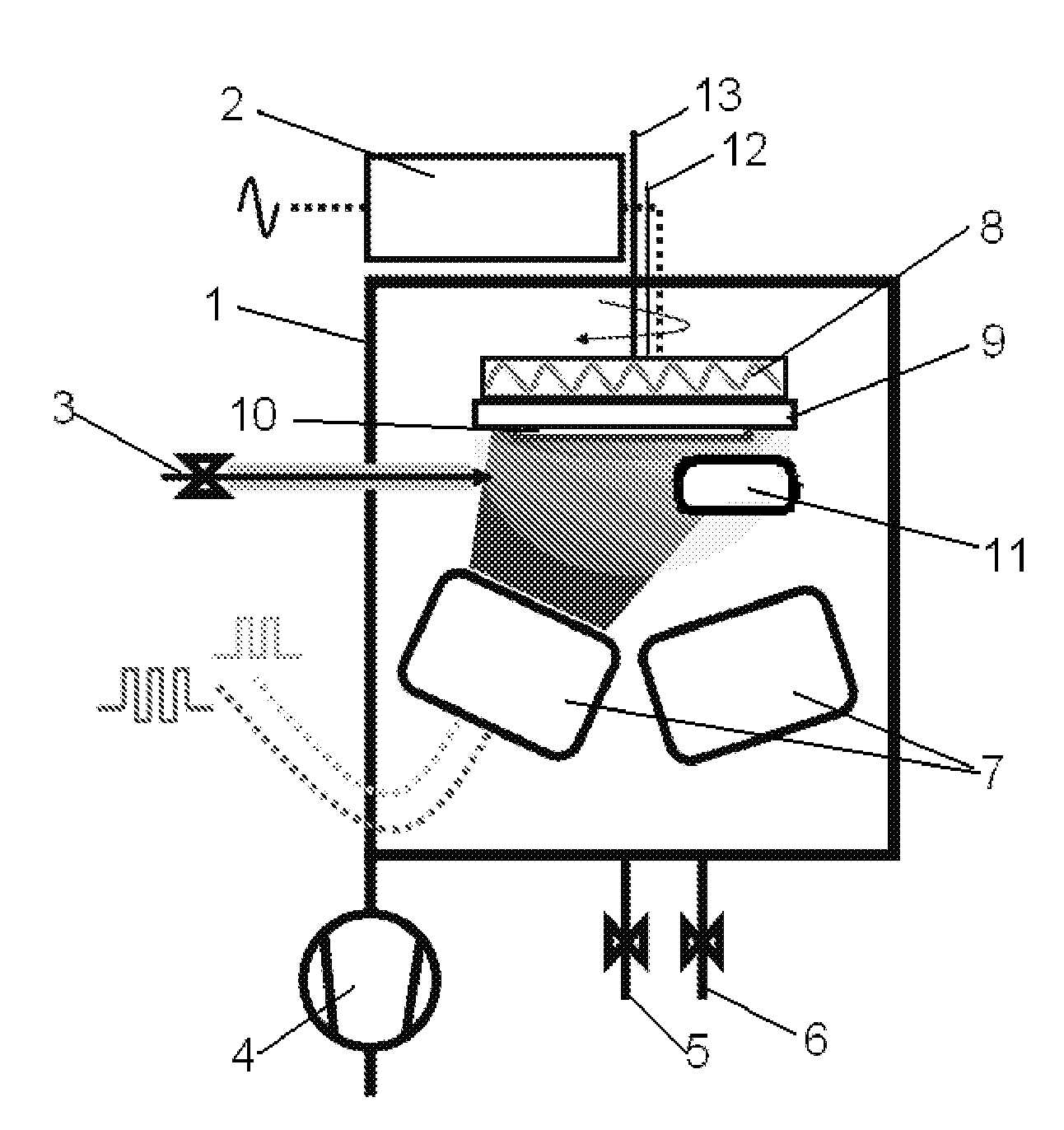
- A combined process using Plasma Enhanced Chemical Vapor Deposition (PECVD) and Physical Vapor Deposition (PVD) techniques to create dielectric and barrier layers, allowing for simultaneous deposition in a single vacuum chamber with independent control of plasma sources, enhancing conformality, thickness, and mechanical stability, and optimizing dielectric breakdown properties.

Method of making dielectric capacitors with increased dielectric breakdown strength
PatentActiveUS20130335882A1
Innovation
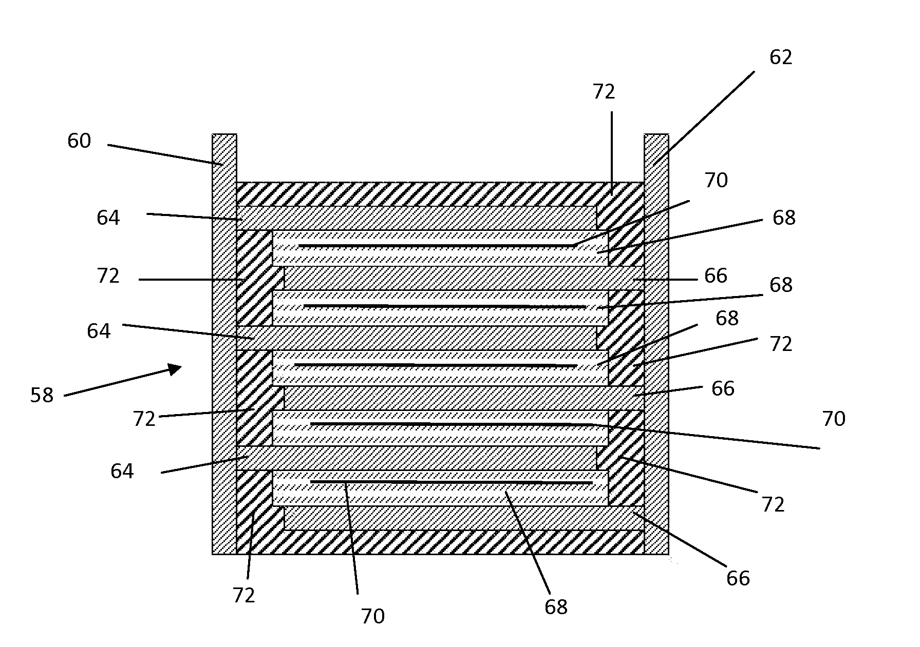
- Embedding thin conductive oxide layers within the ceramic dielectric material matrix to redistribute trapped charge and block the propagation of defects, thereby increasing dielectric breakdown strength and preventing rapid failure.

Safety Standards for Dielectric Systems
The establishment of comprehensive safety standards for dielectric systems represents a critical framework for preventing catastrophic failures associated with dielectric breakdown caused by material defects. These standards encompass multiple layers of protection, from material specifications to operational protocols, ensuring that systems can withstand electrical stress while maintaining operational integrity throughout their service life.
International standards organizations, including IEC, IEEE, and ASTM, have developed rigorous testing protocols specifically addressing defect-related breakdown mechanisms. IEC 60243 series standards define standardized methods for measuring dielectric strength while accounting for the presence of voids, impurities, and manufacturing inconsistencies. These protocols establish minimum performance thresholds that account for statistical variations in material quality and processing conditions.
Material qualification standards mandate comprehensive characterization of dielectric properties under various stress conditions. Standards require manufacturers to demonstrate material performance through accelerated aging tests, partial discharge measurements, and breakdown voltage assessments that specifically target defect-sensitive failure modes. These requirements ensure that materials can withstand operational stresses even when containing typical manufacturing imperfections.
Design safety factors incorporated into standards typically range from 2:1 to 10:1 depending on application criticality and environmental conditions. These factors account for the statistical nature of defect-induced failures and provide adequate margins for unexpected stress concentrations around voids or impurity sites. Critical applications such as power transmission equipment often require higher safety factors due to the severe consequences of dielectric failure.
Quality assurance standards mandate implementation of defect detection and mitigation strategies throughout the manufacturing process. Non-destructive testing requirements, including partial discharge testing and dielectric loss measurements, help identify potentially problematic defects before system deployment. These standards also specify acceptable defect density limits and size thresholds based on extensive reliability data.
Operational safety standards establish monitoring protocols for early detection of degradation processes that could lead to breakdown. Continuous monitoring of partial discharge activity, temperature variations, and dielectric loss changes enables predictive maintenance strategies that prevent catastrophic failures. These standards also define inspection intervals and replacement criteria based on accumulated stress exposure and detected degradation indicators.
Quality Control in Dielectric Manufacturing
Quality control in dielectric manufacturing represents a critical intersection between material science and industrial precision, where the prevention of defects directly correlates with device reliability and performance. The manufacturing process must address three primary defect categories that lead to dielectric breakdown: voids, impurities, and weak points, each requiring distinct detection and mitigation strategies.
Void formation during dielectric manufacturing typically occurs during deposition, curing, or thermal processing stages. Advanced quality control systems employ high-resolution imaging techniques, including scanning electron microscopy and atomic force microscopy, to detect microscopic voids that could compromise dielectric integrity. Real-time monitoring during chemical vapor deposition processes utilizes optical emission spectroscopy to ensure uniform film growth and minimize void nucleation.
Impurity control demands stringent environmental management throughout the manufacturing chain. Clean room protocols with particle counts below Class 10 standards are essential, while chemical purity verification through mass spectrometry and X-ray photoelectron spectroscopy ensures raw material quality. Ion chromatography systems continuously monitor process chemicals, detecting trace contaminants that could migrate into dielectric layers and create conductive pathways.
Weak point identification requires comprehensive electrical testing protocols that simulate operational stress conditions. Time-dependent dielectric breakdown testing applies accelerated voltage and temperature conditions to identify potential failure sites before product deployment. Statistical process control methods analyze breakdown voltage distributions to detect manufacturing variations that could indicate systematic weak point formation.
Modern quality control systems integrate machine learning algorithms to correlate manufacturing parameters with defect formation patterns. These predictive models analyze multi-dimensional data from temperature profiles, pressure variations, and chemical concentrations to optimize process windows and minimize defect probability. Automated optical inspection systems equipped with deep learning capabilities can identify subtle surface anomalies that traditional methods might overlook.
Process validation protocols establish critical control points throughout manufacturing, with in-line monitoring systems providing immediate feedback for process adjustments. Traceability systems track material lots and process conditions, enabling rapid root cause analysis when defects are detected in downstream testing or field applications.
Unlock deeper insights with PatSnap Eureka Quick Research — get a full tech report to explore trends and direct your research. Try now!
Generate Your Research Report Instantly with AI Agent
Supercharge your innovation with PatSnap Eureka AI Agent Platform!