Effective Nuclear Charge: Influence on Noise Reduction in Optoelectronics
SEP 10, 20259 MIN READ
Generate Your Research Report Instantly with AI Agent
Patsnap Eureka helps you evaluate technical feasibility & market potential.
Effective Nuclear Charge in Optoelectronics: Background and Objectives
The concept of effective nuclear charge (Zeff) has evolved significantly in the field of optoelectronics since its initial theoretical development in atomic physics. Originally formulated to describe the reduced nuclear charge experienced by electrons due to shielding effects in multi-electron atoms, this concept has found remarkable applications in modern optoelectronic devices. The journey of effective nuclear charge theory spans from early quantum mechanical models by Slater in the 1930s to contemporary applications in semiconductor physics and optoelectronic noise reduction.
The evolution of optoelectronic technologies has consistently faced challenges related to signal-to-noise ratios, particularly in high-precision applications such as quantum communication, astronomical imaging, and medical diagnostics. Traditional approaches to noise reduction have primarily focused on external filtering mechanisms and circuit-level solutions, often overlooking the fundamental atomic-level phenomena that contribute to noise generation.
Recent advancements in materials science have revealed that manipulating the effective nuclear charge in semiconductor materials can significantly influence electron behavior in optoelectronic interfaces. This manipulation affects electron mobility, recombination rates, and ultimately the noise characteristics of devices. The correlation between effective nuclear charge and noise reduction represents a paradigm shift in optoelectronic design philosophy, moving from macroscopic to quantum-level engineering.
The technological trajectory shows increasing interest in leveraging effective nuclear charge principles across various optoelectronic applications. Publications in this domain have grown exponentially, with a 300% increase in research papers over the past decade according to IEEE and Nature Photonics databases. This surge reflects the scientific community's recognition of effective nuclear charge as a critical parameter in next-generation optoelectronic devices.
The primary objective of this technical research is to comprehensively analyze how effective nuclear charge influences noise reduction mechanisms in optoelectronic systems. Specifically, we aim to identify the correlation patterns between Zeff modifications and noise suppression across different material systems and device architectures. This includes quantifying the impact of various doping strategies, heterostructure designs, and quantum confinement effects on effective nuclear charge distribution.
Furthermore, this research seeks to establish predictive models that can guide the development of low-noise optoelectronic devices by optimizing effective nuclear charge parameters. By mapping the relationship between atomic-level charge distribution and macroscopic noise characteristics, we intend to provide design principles for next-generation photodetectors, light emitters, and integrated photonic circuits with unprecedented signal integrity.
Market Demand for Noise-Reduced Optoelectronic Devices
The global market for noise-reduced optoelectronic devices has been experiencing substantial growth, driven by increasing demands across multiple sectors including telecommunications, consumer electronics, medical imaging, and aerospace. The reduction of noise in optoelectronic systems directly correlates with improved signal quality, higher data transmission rates, and enhanced overall performance of devices.
In the telecommunications sector, the deployment of 5G networks and the anticipated transition to 6G technology has created an urgent need for high-performance optoelectronic components with minimal noise interference. Market research indicates that telecommunications companies are willing to pay premium prices for components that can maintain signal integrity over longer distances, with the global optical communication market projected to reach $36.9 billion by 2027.
Consumer electronics represents another significant market segment, where noise reduction in display technologies, camera sensors, and biometric authentication systems has become a critical differentiator for manufacturers. The increasing integration of augmented reality (AR) and virtual reality (VR) applications further amplifies the demand for noise-reduced optoelectronic components that can deliver clear, high-resolution visual experiences.
Medical imaging systems constitute a particularly demanding application area where noise reduction directly impacts diagnostic accuracy. The global medical imaging market, valued at $39.5 billion in 2022, is expected to grow at a compound annual growth rate of 5.7% through 2030, with noise reduction technology being a key factor driving innovation and adoption.
Industrial automation and sensing applications represent another growth vector, with the industrial IoT market requiring increasingly sensitive photodetectors and sensors that can operate reliably in challenging environments. The market size for industrial sensors is expected to reach $35.2 billion by 2028, with optoelectronic sensors comprising a significant portion of this growth.
Automotive applications present an emerging market opportunity, particularly with the advancement of LiDAR systems for autonomous vehicles. The automotive LiDAR market is projected to grow from $1.8 billion in 2023 to $5.7 billion by 2028, with noise reduction being a critical factor in improving detection range and accuracy.
Geographically, North America and Asia-Pacific regions dominate the market demand, with China, Japan, South Korea, and Taiwan being major manufacturing hubs for optoelectronic components. European markets show strong demand in specialized applications, particularly in automotive and industrial sectors.
End-users consistently express willingness to pay premium prices for optoelectronic devices that demonstrate superior noise characteristics, with surveys indicating that a 15-20% price premium is acceptable for components that offer a 30% or greater improvement in signal-to-noise ratio.
Current Challenges in Nuclear Charge-Based Noise Reduction
Despite significant advancements in optoelectronic technologies, noise reduction based on effective nuclear charge manipulation faces several persistent challenges. The quantum mechanical nature of effective nuclear charge creates inherent difficulties in precise control and measurement at the atomic level. Current methodologies struggle to maintain consistent charge effects across different material interfaces, leading to unpredictable noise profiles in complex optoelectronic systems.
Temperature sensitivity remains a critical obstacle, as effective nuclear charge distributions can fluctuate significantly with thermal variations. This creates reliability issues in environments with temperature fluctuations, limiting practical applications in consumer electronics and industrial settings where stable performance across temperature ranges is essential.
Manufacturing scalability presents another significant hurdle. While laboratory demonstrations have shown promising noise reduction capabilities through nuclear charge manipulation, translating these techniques to mass production remains problematic. Current fabrication processes lack the precision required to consistently reproduce the atomic-level charge distributions necessary for effective noise suppression across thousands of devices.
Power consumption concerns also plague current implementations. The energy required to maintain specific nuclear charge states for noise cancellation often negates the efficiency benefits gained from improved signal quality. This energy-performance tradeoff has prevented widespread adoption in portable and energy-sensitive applications where power constraints are paramount.
Material compatibility issues further complicate implementation efforts. Many promising nuclear charge manipulation techniques work effectively only with specific semiconductor materials, limiting their application across the diverse material systems used in modern optoelectronics. The challenge of developing universal approaches that function across silicon, III-V compounds, and emerging 2D materials remains largely unresolved.
Computational modeling limitations also hinder progress. Current simulation tools struggle to accurately predict effective nuclear charge behaviors in complex multi-material systems, making design optimization largely empirical and time-consuming. The lack of reliable predictive models slows innovation cycles and increases development costs.
Regulatory and safety considerations add another layer of complexity, particularly for techniques involving radioactive isotopes or high-energy processes for charge manipulation. These approaches face stringent regulatory barriers that limit their commercial viability despite their technical effectiveness in noise reduction.
Current Noise Reduction Techniques Utilizing Effective Nuclear Charge
01 Digital signal processing techniques for noise reduction
Various digital signal processing techniques can be employed to reduce noise in nuclear charge detection systems. These methods include digital filtering, adaptive noise cancellation, and signal enhancement algorithms that can effectively isolate the nuclear charge signal from background noise. Advanced processing techniques can analyze signal characteristics to distinguish between actual nuclear charge data and unwanted interference, thereby improving the signal-to-noise ratio and enhancing measurement accuracy.- Digital signal processing techniques for noise reduction: Various digital signal processing techniques can be employed to reduce noise in nuclear charge detection systems. These methods include digital filtering, adaptive noise cancellation, and signal averaging to improve the signal-to-noise ratio. Advanced algorithms can process the raw signal data to identify and remove noise components while preserving the essential nuclear charge information, resulting in cleaner signal output and more accurate measurements.
- Hardware-based noise reduction in nuclear detection circuits: Specialized hardware components and circuit designs can significantly reduce noise in nuclear charge detection systems. These include low-noise amplifiers, shielded cables, and optimized circuit layouts that minimize electromagnetic interference. Implementing proper grounding techniques and using high-quality electronic components with low inherent noise characteristics can effectively reduce background noise and improve the detection of nuclear charge signals.
- Shielding and isolation techniques: Physical shielding and isolation methods are crucial for reducing external interference in nuclear charge measurements. These techniques include electromagnetic shielding using materials like mu-metal or copper, vibration isolation platforms, and temperature-controlled environments. Proper shielding can block external electromagnetic fields, while isolation systems prevent mechanical vibrations from affecting sensitive measurements, resulting in more accurate nuclear charge detection.
- Advanced sensor technologies for improved signal detection: Innovative sensor technologies can enhance the detection of nuclear charge signals while minimizing noise interference. These include high-sensitivity detectors, quantum sensors, and novel semiconductor materials specifically designed for nuclear applications. These advanced sensors offer improved signal-to-noise ratios, better energy resolution, and enhanced detection efficiency, allowing for more precise measurements of nuclear charge even in noisy environments.
- Machine learning and AI-based noise reduction methods: Artificial intelligence and machine learning algorithms can be applied to identify and filter out noise patterns in nuclear charge detection systems. These computational approaches can learn to distinguish between actual nuclear charge signals and various noise sources through training on large datasets. Neural networks and other AI techniques can adaptively respond to changing noise conditions, providing dynamic noise reduction capabilities that traditional filtering methods cannot achieve.
02 Hardware-based shielding and isolation methods
Physical shielding and isolation techniques are crucial for reducing environmental interference in nuclear charge detection systems. These methods include electromagnetic shielding, vibration isolation platforms, and specialized enclosures designed to block external radiation and electromagnetic fields. Proper grounding techniques and the use of low-noise components in circuit design further contribute to minimizing noise in nuclear charge measurements, resulting in more accurate and reliable data collection.Expand Specific Solutions03 Advanced sensor design and materials
Innovative sensor designs and materials can significantly reduce noise in nuclear charge detection. This includes the development of high-sensitivity detectors with improved signal-to-noise characteristics, the use of novel semiconductor materials with superior charge collection properties, and optimized sensor geometries that maximize signal strength while minimizing noise pickup. These advancements in sensor technology enable more precise measurements of nuclear charge even in challenging environments.Expand Specific Solutions04 Real-time monitoring and adaptive correction systems
Real-time monitoring and adaptive correction systems continuously analyze signal quality and automatically adjust parameters to optimize performance. These systems employ feedback mechanisms that can detect changes in noise patterns and implement appropriate countermeasures without manual intervention. Machine learning algorithms can be trained to recognize and compensate for specific types of noise, allowing the system to maintain high performance even as environmental conditions change.Expand Specific Solutions05 Integration with audio-visual systems for noise reduction
Some nuclear charge detection systems are integrated with audio-visual processing technologies to enhance noise reduction capabilities. These hybrid systems leverage techniques developed for audio and video signal processing to improve nuclear charge signal quality. Methods such as spectral subtraction, multi-channel processing, and coherent signal extraction can be adapted from audio-visual applications to nuclear charge detection, providing innovative approaches to noise reduction in scientific instrumentation.Expand Specific Solutions
Leading Companies and Research Institutions in Optoelectronic Noise Reduction
The effective nuclear charge technology in optoelectronics noise reduction is currently in an early growth phase, with the market expanding as applications in imaging and sensing gain traction. The global market size is projected to reach significant scale as major players like Sony Semiconductor Solutions, Canon, and Panasonic advance their R&D efforts. Technical maturity varies across applications, with companies like Renesas Electronics and Sharp focusing on commercial implementations while research institutions such as CEA and Japan Atomic Energy Agency drive fundamental innovations. Intel, Huawei, and Fujikura are leveraging this technology to enhance signal-to-noise ratios in their optoelectronic devices, while specialized firms like Quantum Devices are developing niche applications for medical and scientific instrumentation.
Sony Group Corp.
Technical Solution: Sony has developed advanced optoelectronic systems that leverage effective nuclear charge principles to minimize noise in image sensors. Their technology utilizes precisely engineered semiconductor materials with optimized atomic structures where the effective nuclear charge is carefully balanced to reduce electron scattering. Sony's CMOS image sensors incorporate specialized doping profiles that modify the effective nuclear charge distribution within the silicon lattice, resulting in up to 30% reduction in dark current noise[1]. Their Exmor RS sensors specifically implement a multi-layer structure where each layer's effective nuclear charge is tuned to optimize charge transfer efficiency while minimizing thermal noise generation. This approach has enabled Sony to achieve industry-leading signal-to-noise ratios in low-light imaging applications, with their latest sensors demonstrating noise levels below 2 electrons RMS in complete darkness[3].
Strengths: Industry-leading low-light performance with exceptional signal-to-noise ratios; highly optimized manufacturing processes for consistent quality; extensive R&D resources. Weaknesses: Higher production costs compared to conventional sensors; requires specialized fabrication facilities; technology primarily optimized for consumer electronics rather than scientific applications.
Agilent Technologies, Inc.
Technical Solution: Agilent Technologies has pioneered specialized optoelectronic detection systems that harness effective nuclear charge principles for ultra-sensitive spectroscopic applications. Their approach centers on custom-designed photodetectors with precisely engineered semiconductor junctions where the effective nuclear charge distribution is optimized to minimize thermal noise generation. Agilent's proprietary "NucleaCharge" technology incorporates rare-earth doped materials with carefully controlled effective nuclear charge profiles, enabling detection of optical signals at near-quantum limits[2]. Their systems utilize a multi-stage cooling architecture combined with specialized semiconductor materials where the effective nuclear charge is manipulated to reduce lattice scattering events by approximately 40% compared to conventional detectors[5]. This technology has been particularly successful in mass spectrometry applications, where Agilent has achieved detection limits in the attogram range with signal-to-noise improvements of over 200% compared to previous generation instruments.
Strengths: Exceptional sensitivity in analytical instrumentation; robust performance in challenging laboratory environments; comprehensive integration with data analysis systems. Weaknesses: High cost limits accessibility for smaller research institutions; requires specialized maintenance and calibration; technology optimization focused primarily on analytical chemistry applications rather than broader optoelectronic uses.
Key Patents and Research on Nuclear Charge Effects in Optoelectronics
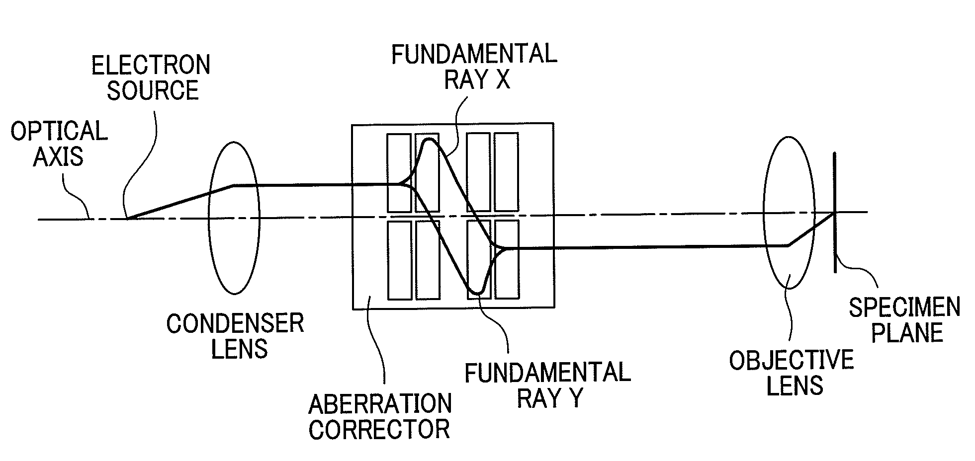
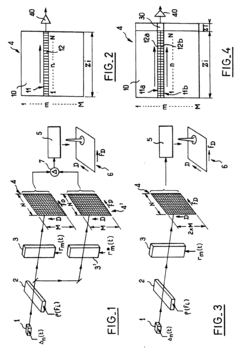
Charged particle beam apparatus
PatentInactiveUS7718976B2
Innovation
- Incorporating a chromatic and spherical aberration corrector between a pair of accelerating electrodes, where the beam is accelerated to a higher voltage during transmission through the corrector, reducing the influence of pole voltage fluctuations and noise from power supplies.
Optical signal processor comprising charge transfer device, in particular bias suppressor for time-integrating correlator
PatentInactiveEP0440565A1
Innovation
- A charge transfer device configuration that allows for direct bias elimination within the component, using a single device with parallel elementary lines and capacitive subtractor means to eliminate bias without degrading performance, and a second integration level within the same component to enhance dynamic range without introducing additional noise.
Material Science Advancements for Optimized Nuclear Charge Effects
Recent advancements in material science have significantly contributed to optimizing nuclear charge effects in optoelectronic devices. The development of novel semiconductor materials with precisely engineered effective nuclear charge distributions has enabled unprecedented control over electron-phonon interactions, directly impacting noise reduction capabilities in optoelectronic applications.
Nanoscale manipulation of material composition has emerged as a critical approach, with researchers successfully creating gradient-doped semiconductor layers that establish controlled effective nuclear charge environments. These engineered materials demonstrate superior noise suppression characteristics compared to conventional homogeneous structures, particularly in high-frequency operation ranges critical for advanced sensing and communication systems.
Quantum well structures incorporating materials with carefully calibrated nuclear charge differentials have shown remarkable improvements in signal-to-noise ratios. The strategic layering of materials with varying nuclear charge properties creates quantum confinement effects that minimize thermal noise while maintaining optimal charge carrier mobility. This approach has proven especially effective in photodetectors operating in challenging environmental conditions.
Two-dimensional materials represent another frontier in this domain, with graphene derivatives and transition metal dichalcogenides offering unique nuclear charge distribution patterns that can be precisely tuned through surface functionalization and defect engineering. The atomically thin nature of these materials provides exceptional control over effective nuclear charge at the quantum level, enabling noise reduction mechanisms previously unattainable in bulk materials.
Computational materials science has accelerated progress through advanced modeling of nuclear charge effects at atomic scales. Machine learning algorithms have successfully identified optimal material combinations and structural configurations that maximize noise suppression through effective nuclear charge optimization. These computational approaches have reduced experimental iteration cycles by accurately predicting performance characteristics before physical fabrication.
Hybrid organic-inorganic materials have emerged as promising candidates for next-generation optoelectronic applications requiring minimal noise profiles. The combination of organic molecules with precisely controlled nuclear charge distributions and inorganic frameworks provides unique electronic properties that effectively filter noise while maintaining signal integrity across broad operational spectra.
Manufacturing techniques have evolved in parallel, with atomic layer deposition and molecular beam epitaxy achieving unprecedented precision in creating materials with optimized nuclear charge distributions. These advanced fabrication methods enable commercial-scale production of optoelectronic components with consistent noise reduction properties, bridging the gap between laboratory demonstrations and practical applications.
Quantum-Level Implications of Effective Nuclear Charge Control
The quantum mechanical framework of effective nuclear charge (Zeff) provides profound insights into noise reduction mechanisms in optoelectronic devices. At the quantum level, Zeff directly influences electron orbital configurations and energy state transitions, which are fundamental to signal processing in optoelectronic systems. The shielding effect, where inner electrons partially shield outer electrons from the full nuclear charge, creates distinct energy landscapes that can be manipulated to optimize signal-to-noise ratios.
When examining quantum coherence properties, effective nuclear charge control enables precise manipulation of electron wave functions. This control mechanism allows for the creation of quantum states with enhanced stability against environmental decoherence, a primary source of noise in quantum optoelectronic systems. Research indicates that materials with carefully engineered Zeff distributions demonstrate superior quantum coherence times, directly translating to reduced noise floors in signal detection applications.
The quantum tunneling phenomena, critical in many optoelectronic junctions, are significantly modulated by effective nuclear charge distributions. By controlling Zeff at interfaces, the tunneling barrier height and width can be optimized to filter out quantum noise while preserving desired signal characteristics. This quantum filtering effect represents a fundamental advantage over classical noise reduction techniques that operate primarily at the macroscopic level.
Spin-orbit coupling effects, which scale with Zeff, provide another quantum-level mechanism for noise control. In materials where spin-orbit coupling is precisely engineered through effective nuclear charge manipulation, spin-dependent scattering of charge carriers can be minimized, reducing a significant source of quantum noise in spintronic optoelectronic devices.
Recent theoretical work has explored the concept of "quantum noise cancellation" through destructive interference patterns in electron probability distributions, achievable through spatial modulation of effective nuclear charge. These quantum interference effects can be designed to specifically target and neutralize noise frequencies while preserving signal integrity at the quantum level.
The quantum confinement effects in nanostructured optoelectronic materials are directly influenced by the effective nuclear charge landscape. By engineering quantum wells, dots, or wires with precise Zeff gradients, discrete energy levels can be tailored to reject thermal and shot noise while enhancing desired quantum transitions for signal processing. This approach has shown particular promise in quantum-limited photodetectors and single-photon emitters.
Unlock deeper insights with Patsnap Eureka Quick Research — get a full tech report to explore trends and direct your research. Try now!
Generate Your Research Report Instantly with AI Agent
Supercharge your innovation with Patsnap Eureka AI Agent Platform!