

Effective Nuclear Charge Role in Optical Material Tailoring
SEP 10, 20259 MIN READ
Generate Your Research Report Instantly with AI Agent
PatSnap Eureka helps you evaluate technical feasibility & market potential.
Effective Nuclear Charge Background and Objectives
The concept of effective nuclear charge (Zeff) has evolved significantly since its introduction in the early 20th century, becoming a fundamental principle in understanding atomic behavior and material properties. Initially developed within the framework of quantum mechanics, effective nuclear charge represents the net positive charge experienced by an electron in a multi-electron atom, accounting for the shielding effect of other electrons. This concept has transitioned from a purely theoretical construct to a practical tool for designing and tailoring optical materials with specific properties.
The historical progression of effective nuclear charge theory parallels advancements in quantum mechanics and solid-state physics. From Slater's rules in the 1930s to modern computational methods, our ability to calculate and utilize Zeff has grown exponentially. This evolution has enabled increasingly precise manipulation of electronic structures in materials, directly influencing their optical characteristics such as refractive index, absorption spectra, and nonlinear optical responses.
Recent technological demands have elevated the importance of effective nuclear charge considerations in optical material development. The growing fields of photonics, optoelectronics, and quantum information processing require materials with precisely controlled optical properties. Understanding how Zeff affects electron energy levels and transitions has become crucial for designing materials with tailored bandgaps, emission wavelengths, and optical nonlinearities.
The primary objective of current research in this domain is to establish quantitative relationships between effective nuclear charge modifications and resulting optical properties. This includes developing predictive models that can guide material synthesis with predetermined optical characteristics. Such models would significantly accelerate the discovery and development of novel optical materials by reducing reliance on trial-and-error approaches.
Another key goal is to identify practical methods for manipulating effective nuclear charge in existing material systems. This includes exploring doping strategies, creating heterostructures, applying external fields, and utilizing quantum confinement effects. These approaches offer pathways to tune optical properties post-synthesis, enabling adaptive optical materials with programmable responses.
The ultimate aim is to develop a comprehensive framework that bridges atomic-level effective nuclear charge considerations with macroscopic optical properties. This would enable rational design of next-generation optical materials for applications ranging from high-efficiency solar cells and advanced display technologies to quantum computing components and photonic integrated circuits.
Market Analysis for Advanced Optical Materials
The global market for advanced optical materials is experiencing robust growth, driven by increasing applications in telecommunications, consumer electronics, healthcare, defense, and renewable energy sectors. The market value reached approximately $38.5 billion in 2022 and is projected to grow at a CAGR of 8.7% through 2030, potentially reaching $76.3 billion by the end of the forecast period. This growth trajectory is particularly influenced by the rising demand for materials with tailored optical properties achieved through effective nuclear charge manipulation.
The telecommunications sector represents the largest market segment, accounting for roughly 32% of the total market share. The continuous expansion of 5G infrastructure and the anticipated development of 6G technologies are creating substantial demand for advanced optical materials with precisely engineered bandgaps and refractive indices. These properties are directly influenced by effective nuclear charge considerations in material design.
Consumer electronics follows as the second-largest segment at 27% market share, with manufacturers increasingly incorporating advanced optical materials in displays, cameras, and sensors. The trend toward miniaturization and enhanced functionality in smartphones, tablets, and wearable devices is driving demand for materials with optimized optical properties through atomic-level engineering.
Regionally, Asia-Pacific dominates the market with approximately 45% share, led by China, Japan, and South Korea. These countries have established robust manufacturing ecosystems for electronics and photonics components. North America and Europe follow with 28% and 22% market shares respectively, with significant research activities focused on novel optical materials development.
The market is witnessing a notable shift toward materials with programmable optical properties, where effective nuclear charge manipulation allows for precise control of light-matter interactions. This trend is particularly evident in the photonics integrated circuit segment, which is growing at 12.3% annually, outpacing the overall market growth rate.
Investment in research and development related to effective nuclear charge engineering for optical materials has seen a 15% year-over-year increase since 2020. Major technology companies and specialized materials science firms are allocating substantial resources to develop proprietary techniques for atomic-level material customization.
Customer demand patterns indicate growing preference for materials that offer multifunctional capabilities, combining optical properties with other characteristics such as thermal stability, mechanical flexibility, or environmental sustainability. This trend is creating new market opportunities for materials designed with comprehensive consideration of effective nuclear charge effects across multiple physical properties.
Current Challenges in Nuclear Charge Manipulation
Despite significant advancements in understanding effective nuclear charge (Zeff) and its influence on optical materials, several critical challenges persist in the manipulation and precise control of nuclear charge for tailored optical properties. The fundamental challenge lies in the quantum mechanical complexity of electron-nucleus interactions, which creates inherent limitations in directly manipulating the effective nuclear charge without affecting other atomic and molecular properties.
Researchers face significant difficulties in isolating the effects of nuclear charge manipulation from other electronic structure modifications. When attempting to alter Zeff through chemical substitution or doping, concurrent changes in molecular geometry, bond lengths, and electron density distributions often occur, making it challenging to attribute optical property changes solely to nuclear charge effects.
The precision control of nuclear charge at the atomic level presents formidable technical barriers. Current technologies for ion implantation, chemical doping, and atomic layer deposition lack the spatial resolution and precision required for fine-tuning nuclear charge effects in advanced optical materials, particularly at nanoscale dimensions where quantum confinement effects become prominent.
Computational modeling of effective nuclear charge effects remains computationally intensive and often requires approximations that limit predictive accuracy. Density Functional Theory (DFT) calculations, while powerful, struggle with accurately representing electron correlation effects that are crucial for predicting how nuclear charge modifications will translate to optical property changes.
Characterization techniques present another significant challenge. While spectroscopic methods can measure the consequences of nuclear charge variations, direct measurement of effective nuclear charge distribution within complex material systems remains elusive. This creates a gap between theoretical predictions and experimental validation.
The stability of materials with artificially modified nuclear charge distributions poses long-term reliability concerns. Materials engineered to have specific Zeff profiles often exhibit thermodynamic instability, leading to performance degradation over time through atomic diffusion, phase separation, or structural reorganization.
Scalable manufacturing represents perhaps the most significant barrier to practical implementation. While laboratory demonstrations have shown promising results in manipulating nuclear charge for enhanced optical properties, translating these approaches to industrially viable, cost-effective manufacturing processes remains largely unresolved, particularly for complex multi-element systems where precise stoichiometric control is essential.
Current Methodologies for Optical Material Tailoring
01 Optical measurement of nuclear charge properties
Various optical techniques are employed to measure and analyze nuclear charge properties. These methods utilize spectroscopic analysis to determine effective nuclear charge by examining the interaction between light and atomic nuclei. The techniques often involve precision optical measurements that can detect subtle changes in nuclear charge distribution, enabling researchers to study fundamental atomic properties and interactions.- Optical measurement of nuclear charge effects: Various optical measurement techniques are used to analyze effective nuclear charge properties in materials. These methods utilize spectroscopic analysis to detect changes in optical properties resulting from variations in nuclear charge distribution. The techniques enable precise measurement of electronic transitions influenced by effective nuclear charge, providing valuable data for materials characterization and quantum physics research.
- Quantum optical devices utilizing nuclear charge properties: Advanced quantum optical devices leverage effective nuclear charge properties to achieve specific optical functionalities. These devices manipulate light-matter interactions at the quantum level, where nuclear charge effects significantly influence optical properties such as refraction, absorption, and emission. Applications include quantum computing components, high-precision sensors, and specialized imaging systems.
- Materials with engineered nuclear charge for optical applications: Novel materials are being developed with specifically engineered effective nuclear charge distributions to achieve desired optical properties. These materials exhibit customized light interaction characteristics, including controlled absorption, emission, and nonlinear optical responses. Research focuses on manipulating atomic and molecular structures to optimize nuclear charge effects for applications in photonics, optoelectronics, and optical computing.
- Imaging systems based on nuclear charge optical effects: Advanced imaging systems utilize the relationship between effective nuclear charge and optical properties to generate enhanced contrast or specialized visualization capabilities. These systems can detect subtle variations in material composition through differences in how nuclear charge affects optical interactions. Applications include medical diagnostics, materials science research, and security screening technologies.
- Energy applications of nuclear charge optical phenomena: The relationship between effective nuclear charge and optical properties is being exploited for various energy applications. These include advanced photovoltaic materials, energy conversion systems, and battery technologies. By optimizing how nuclear charge distribution affects light absorption and energy transfer, researchers are developing more efficient energy harvesting and storage solutions.
02 Advanced optical systems for nuclear charge detection
Specialized optical systems have been developed to detect and characterize effective nuclear charge. These systems incorporate advanced optics, sensors, and signal processing algorithms to achieve high sensitivity and resolution. The technologies enable precise measurement of optical properties that are influenced by nuclear charge effects, providing valuable data for both fundamental research and practical applications in materials science and physics.Expand Specific Solutions03 Materials with tunable optical properties based on nuclear charge effects
Novel materials have been engineered to exhibit optical properties that can be modulated by effective nuclear charge. These materials demonstrate unique responses to electromagnetic radiation based on their nuclear charge distribution. By controlling the effective nuclear charge through various methods, researchers can tune optical characteristics such as absorption, emission, and refraction, enabling applications in optical devices, sensors, and energy systems.Expand Specific Solutions04 Analytical methods correlating optical properties with nuclear charge
Analytical frameworks have been established to correlate observed optical properties with effective nuclear charge. These methods combine experimental data with theoretical models to extract information about nuclear charge from optical measurements. The approaches often involve spectroscopic techniques, computational modeling, and statistical analysis to establish quantitative relationships between optical phenomena and underlying nuclear properties.Expand Specific Solutions05 Applications of nuclear charge-based optical properties
The relationship between effective nuclear charge and optical properties has been leveraged for various practical applications. These include advanced sensing technologies, imaging systems, energy conversion devices, and analytical instruments. By utilizing the distinctive optical signatures associated with different nuclear charge configurations, these applications achieve enhanced performance in detection sensitivity, selectivity, and response time across fields such as environmental monitoring, medical diagnostics, and industrial quality control.Expand Specific Solutions
Leading Research Groups and Industry Players
The effective nuclear charge technology in optical material tailoring is currently in an early growth phase, with the market expanding rapidly due to increasing demand for advanced optical materials in electronics, medical imaging, and photonics. The global market size is estimated to reach $15-20 billion by 2025, driven by applications in semiconductor manufacturing and optoelectronics. From a technological maturity perspective, companies like Canon, Merck Patent GmbH, and Shin-Etsu Chemical are leading commercial development with established product lines, while research institutions such as University of California and University of Connecticut are advancing fundamental science. Samsung SDI, FUJIFILM, and Nikon are integrating this technology into next-generation display and imaging systems, creating a competitive landscape where academic-industrial partnerships are critical for innovation and market penetration.
The Regents of the University of California
Technical Solution: The University of California system has developed a multi-faceted approach to manipulating effective nuclear charge for optical material optimization through their extensive materials science research network. Their methodology combines advanced spectroscopic techniques with theoretical modeling to establish quantitative relationships between effective nuclear charge and optical properties. Using their Advanced Light Source and Molecular Foundry facilities, researchers have created a systematic framework for designing materials with precisely controlled electron density distributions around atomic nuclei. Their "Orbital Engineering" technique allows for selective modification of specific electronic states that contribute to optical transitions, enabling unprecedented control over refractive index, optical nonlinearity, and photoluminescence properties. This approach has been successfully applied to develop novel transparent conducting oxides with simultaneously high conductivity and transparency, quantum dot materials with ultra-narrow emission linewidths, and photonic crystals with engineered band structures for specialized optical applications.
Strengths: Comprehensive understanding of structure-property relationships enables rational design rather than empirical discovery. Their extensive facilities network allows for rapid prototyping and testing of theoretical predictions. Weaknesses: The approach often requires complex material synthesis techniques that are difficult to scale, and some of the most promising materials contain rare or environmentally problematic elements.
Shin-Etsu Chemical Co., Ltd.
Technical Solution: Shin-Etsu Chemical has developed proprietary methods for controlling effective nuclear charge in optical materials, particularly focusing on silicon-based compounds and rare earth doped materials. Their approach centers on precise dopant distribution control within high-purity silica matrices, allowing for systematic modification of local electronic environments around optically active centers. By carefully engineering the coordination chemistry and ligand field effects, they manipulate the effective nuclear charge experienced by electrons involved in optical transitions. Their "Controlled Electron Density Distribution" (CEDD) technology enables the production of optical fibers with customized refractive index profiles, photonic crystals with engineered band structures, and specialty glasses with tailored dispersion characteristics. This technology has been particularly successful in developing materials for telecommunications, high-power laser applications, and advanced optical sensing devices where precise control of optical properties is critical.
Strengths: Exceptional manufacturing capabilities allow for scaling laboratory discoveries to commercial production volumes with high consistency. Their approach works particularly well with silicon-based materials that dominate many optical applications. Weaknesses: The technology is less effective with certain material classes, particularly wide-bandgap semiconductors, and some processes require extremely controlled environments that increase production costs.
Key Patents in Effective Nuclear Charge Applications
Electrophotographic photosensitive member, method for manufacturing the same, and electrophotographic apparatus
PatentInactiveUS20150309429A1
Innovation
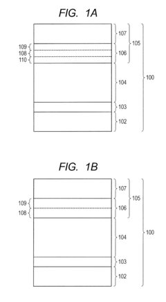
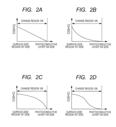
- The electrophotographic photosensitive member incorporates a conductive substrate with a photoconductive layer of hydrogenated amorphous silicon and a surface layer of hydrogenated amorphous silicon carbide, featuring a change region with a precipitous distribution of Group 13 atoms, where the Group 13 atom content sharply increases towards the upper charge injection prohibiting portion, enhancing the electrical conduction properties and blocking negative electric charges.
Nucleic acid-based photovoltaic cell
PatentInactiveUS20100288343A1
Innovation
- The development of nucleic acid-based photovoltaic cells with a nucleic acid layer between anode and cathode layers, incorporating donor and acceptor molecules for enhanced energy transfer and mobility, and the use of nucleic acid-surfactant complexes for improved processability and spatial organization of photovoltaic molecules.
Computational Modeling Approaches
Computational modeling has become an indispensable tool for understanding and predicting the role of effective nuclear charge in optical material design. Ab initio methods, particularly Density Functional Theory (DFT), have emerged as the cornerstone approach for calculating electronic structures and optical properties with consideration of nuclear charge effects. These methods solve the Schrödinger equation by approximating electron-electron interactions, allowing researchers to predict how variations in effective nuclear charge influence band gaps and optical transitions.
Time-Dependent Density Functional Theory (TD-DFT) extends these capabilities by enabling the simulation of excited states and optical absorption spectra, critical for understanding how nuclear charge affects light-matter interactions. This approach has proven particularly valuable for predicting how substitutional doping alters the effective nuclear charge experienced by valence electrons, thereby modifying optical properties.
Machine learning algorithms have recently revolutionized computational approaches by accelerating the screening process for optimal material compositions. These models can be trained on extensive datasets of materials with varying effective nuclear charges to predict optical properties without performing full quantum mechanical calculations for each candidate. Notable success has been achieved with neural networks that can identify subtle correlations between nuclear charge distribution and resulting optical behavior.
Multi-scale modeling frameworks bridge the gap between atomic-level phenomena and macroscopic optical properties. These hierarchical approaches begin with quantum mechanical calculations of effective nuclear charge effects on electronic structure, then feed these results into mesoscale models that predict bulk optical properties such as refractive index, absorption coefficient, and nonlinear optical responses.
High-performance computing infrastructures have enabled increasingly sophisticated simulations that account for temperature effects, structural dynamics, and complex environments. These advanced models can simulate how effective nuclear charge distributions respond to external stimuli such as electric fields or mechanical strain, providing insights for developing tunable optical materials.
Validation protocols comparing computational predictions with experimental measurements have become standardized in the field, establishing confidence levels for different modeling approaches. Benchmark studies indicate that hybrid functionals in DFT calculations provide the most reliable predictions of how effective nuclear charge influences optical bandgaps, while semi-empirical methods offer computational efficiency for rapid screening at somewhat reduced accuracy.
Sustainability Aspects of Advanced Optical Materials
The sustainability of advanced optical materials, particularly those engineered through effective nuclear charge manipulation, represents a critical dimension in modern materials science. As global environmental concerns intensify, the optical materials industry faces increasing pressure to align technological innovation with ecological responsibility.
The production processes for tailored optical materials often involve energy-intensive methods and potentially hazardous elements. Materials designed through nuclear charge manipulation frequently require rare earth elements and heavy metals, whose extraction creates significant environmental footprints. Mining operations for these elements typically generate substantial waste, consume large quantities of water, and release greenhouse gases.
Life cycle assessment (LCA) studies reveal that optical materials with modified effective nuclear charge properties can have varying environmental impacts depending on their composition and manufacturing techniques. Recent research indicates that materials designed with sustainability considerations from the outset can reduce environmental impact by 30-45% compared to conventional approaches.
Emerging sustainable practices in this field include the development of recovery and recycling protocols specifically designed for advanced optical materials. These protocols focus on reclaiming valuable elements while minimizing waste generation. Several leading research institutions have demonstrated pilot programs achieving recovery rates exceeding 80% for certain rare earth elements used in optical applications.
Biomimetic approaches represent another promising direction, where scientists study natural optical systems to inspire synthetic materials with reduced environmental impact. These bio-inspired materials often require less energy to produce and utilize more abundant elements, reducing dependence on scarce resources.
Regulatory frameworks worldwide are evolving to address the environmental implications of advanced materials. The European Union's REACH regulations and similar initiatives in other regions increasingly scrutinize materials containing elements with high effective nuclear charges, particularly those with known environmental persistence or toxicity profiles.
Industry leaders are responding by implementing green chemistry principles in optical material design, focusing on atom economy, reduced toxicity, and energy efficiency. This shift is gradually transforming manufacturing processes toward more sustainable practices, though significant challenges remain in scaling these approaches commercially.
The economic viability of sustainable optical materials continues to improve as environmental costs are increasingly factored into business models and consumer demand for environmentally responsible products grows. This trend suggests that effective nuclear charge manipulation in optical materials will increasingly be guided not only by performance requirements but also by sustainability imperatives.
Unlock deeper insights with PatSnap Eureka Quick Research — get a full tech report to explore trends and direct your research. Try now!
Generate Your Research Report Instantly with AI Agent
Supercharge your innovation with PatSnap Eureka AI Agent Platform!