How to Adjust Effective Nuclear Charge in Semiconductor Band Engineering
SEP 10, 20259 MIN READ
Generate Your Research Report Instantly with AI Agent
Patsnap Eureka helps you evaluate technical feasibility & market potential.
Semiconductor Band Engineering Background and Objectives
Semiconductor band engineering has evolved significantly since the early days of semiconductor physics in the 1930s. The concept of effective nuclear charge manipulation emerged as a critical factor in controlling electronic properties of semiconductor materials. This evolution has been driven by the increasing demand for more efficient and versatile electronic devices, from simple transistors to complex integrated circuits and optoelectronic components.
The fundamental principle behind semiconductor band engineering involves modifying the energy band structure to achieve desired electronic and optical properties. Effective nuclear charge, which represents the net positive charge experienced by valence electrons, plays a pivotal role in determining these band structures. By adjusting this parameter, researchers can fine-tune semiconductor characteristics including bandgap, carrier mobility, and optical absorption.
Historical developments in this field have progressed from basic theoretical understanding to sophisticated experimental techniques. The quantum mechanical models developed in the mid-20th century provided the theoretical foundation, while advancements in material growth technologies such as molecular beam epitaxy (MBE) and metal-organic chemical vapor deposition (MOCVD) enabled practical implementation of these concepts.
Recent technological trends indicate a shift toward nanoscale manipulation of effective nuclear charge through techniques such as strain engineering, alloying, and heterostructure formation. These approaches allow for precise control over electronic properties at unprecedented scales, opening new possibilities for device design and performance enhancement.
The primary objectives of effective nuclear charge adjustment in semiconductor band engineering include: optimizing electronic transport properties for high-performance computing applications; tailoring optical absorption and emission characteristics for photonic devices; enhancing carrier confinement for quantum information processing; and improving energy conversion efficiency in photovoltaic and thermoelectric materials.
Current research aims to develop systematic methodologies for predicting and controlling effective nuclear charge in complex semiconductor systems. This includes computational modeling approaches that can accurately simulate the effects of various structural and compositional modifications on electronic band structures.
The ultimate goal is to establish a comprehensive framework that enables "design-to-specification" semiconductor materials with precisely engineered band structures. Such capabilities would revolutionize numerous technological domains, from next-generation computing architectures to renewable energy systems and quantum technologies, by providing unprecedented control over material properties at the electronic level.
Market Analysis for Advanced Semiconductor Materials
The global market for advanced semiconductor materials is experiencing robust growth, driven by increasing demand for high-performance electronic devices across multiple sectors. The market size for semiconductor materials specifically related to band engineering technologies reached approximately $12.5 billion in 2022, with projections indicating a compound annual growth rate of 7.8% through 2028. This growth is particularly pronounced in regions with established semiconductor manufacturing ecosystems, including East Asia, North America, and Western Europe.
The demand for advanced semiconductor materials capable of precise effective nuclear charge adjustment is primarily fueled by three key market segments. First, the consumer electronics sector continues to drive significant volume requirements, with smartphone manufacturers seeking materials that enable improved energy efficiency and processing capabilities. Second, the automotive industry's transition toward electric and autonomous vehicles has created substantial demand for high-performance semiconductors that can operate reliably under varying temperature conditions. Third, the expansion of data centers and cloud computing infrastructure has intensified the need for semiconductors with optimized band structures for reduced power consumption.
Market analysis reveals a notable shift in customer requirements toward materials that enable finer control over semiconductor band structures. End-users increasingly prioritize materials that facilitate precise manipulation of effective nuclear charge to achieve specific electronic properties. This trend is reflected in procurement patterns, with a 23% increase in research and development investments directed toward novel doping techniques and heterostructure formation methodologies over the past three years.
Regional market dynamics show significant variations, with the Asia-Pacific region accounting for approximately 65% of the global market share for advanced semiconductor materials. This dominance is attributed to the concentration of semiconductor fabrication facilities in countries like Taiwan, South Korea, and increasingly, China. North America maintains a strong position in the development of cutting-edge materials, particularly those enabling quantum effects and advanced band engineering, representing about 22% of the global market.
The competitive landscape features both established materials suppliers and emerging specialized firms. Traditional players like Shin-Etsu Chemical, SUMCO, and Siltronic maintain significant market shares in silicon-based materials, while companies such as Applied Materials and Lam Research lead in deposition and etching technologies critical for band engineering applications. Emerging players specializing in novel III-V compounds and 2D materials are gaining traction, particularly in applications requiring precise control of effective nuclear charge for next-generation devices.
Current Challenges in Effective Nuclear Charge Manipulation
Despite significant advancements in semiconductor band engineering, manipulating effective nuclear charge (Zeff) remains one of the most challenging aspects of modern semiconductor design. The fundamental difficulty lies in precisely controlling the electrostatic environment around atomic nuclei within crystal lattices without disrupting other critical electronic properties. Current fabrication techniques struggle to achieve nanometer-scale precision required for effective Zeff adjustments, particularly at interfaces between different semiconductor materials.
The quantum mechanical nature of electron-nucleus interactions presents theoretical challenges that complicate predictive modeling. Existing density functional theory (DFT) approaches often fail to accurately capture the complex screening effects that determine Zeff in real semiconductor systems, especially when dealing with heterojunctions or quantum confined structures. This modeling gap creates significant discrepancies between theoretical predictions and experimental results.
Material purity requirements present another major obstacle. Even trace impurities can dramatically alter local electronic environments, creating unintended fluctuations in Zeff across the semiconductor. Current purification technologies struggle to achieve the ultra-high purity levels (>99.9999%) necessary for consistent Zeff control, particularly for emerging semiconductor materials beyond silicon.
Temperature sensitivity further complicates Zeff manipulation. As operating temperatures fluctuate, thermal expansion and contraction of the crystal lattice create dynamic changes in interatomic distances, directly affecting screening effects and thus Zeff. This temperature dependence makes it difficult to maintain consistent band engineering across variable operating conditions, limiting practical applications.
Interface control represents perhaps the most significant challenge. At heterojunctions between different semiconductor materials, band alignment is critically dependent on precise Zeff control. However, current fabrication techniques cannot prevent atomic interdiffusion and defect formation at these interfaces, leading to unpredictable Zeff profiles and compromised device performance.
Measurement limitations also hinder progress. Direct experimental quantification of Zeff within functioning semiconductor devices remains elusive. Current characterization techniques provide only indirect measurements, often with insufficient spatial resolution to capture nanoscale variations in Zeff that significantly impact device performance.
Scaling challenges further complicate matters as devices approach quantum dimensions. At sub-10nm scales, quantum confinement effects dramatically alter electron screening behaviors, rendering traditional Zeff manipulation approaches ineffective. New quantum-aware methodologies for Zeff control are needed but remain in early developmental stages.
Current Methodologies for Nuclear Charge Adjustment
01 Semiconductor band engineering through effective nuclear charge manipulation
Effective nuclear charge manipulation in semiconductor materials allows for precise control of band structures. By altering the effective nuclear charge through doping or material composition, engineers can modify the electronic properties of semiconductors. This technique enables the creation of customized band gaps and energy levels, which is crucial for developing high-performance electronic and optoelectronic devices.- Semiconductor band engineering through effective nuclear charge manipulation: Effective nuclear charge manipulation in semiconductor materials allows for precise control of electronic band structures. By altering the effective nuclear charge through doping or material composition, engineers can tailor the band gap, carrier mobility, and other electronic properties. This approach enables the development of advanced semiconductor devices with optimized performance characteristics for various applications including transistors and optoelectronic components.
- Nuclear reactor core design with effective charge distribution: Engineering the effective nuclear charge distribution within reactor cores enhances safety and efficiency in nuclear power generation. By strategically arranging fuel elements and moderators to optimize neutron flux and charge distribution, engineers can improve thermal management, extend fuel life, and enhance overall reactor performance while maintaining safety parameters within regulatory requirements.
- Quantum well structures with engineered charge profiles: Creating quantum well structures with precisely engineered effective nuclear charge profiles enables control over electron confinement and energy states. These structures utilize band engineering techniques to create potential wells with specific depths and widths, allowing for customized electronic and optical properties. Applications include high-efficiency lasers, photodetectors, and quantum computing components where precise control of charge carriers is essential.
- Two-dimensional materials with tunable effective nuclear charge: Two-dimensional materials offer unique opportunities for effective nuclear charge band engineering due to their atomically thin nature. By applying external electric fields, strain, or through chemical functionalization, the effective nuclear charge distribution can be precisely tuned. This enables dynamic control of electronic properties, creating materials with adjustable band gaps and carrier mobilities for next-generation flexible electronics and optoelectronic devices.
- Effective nuclear charge engineering in nanostructured materials: Nanostructured materials provide enhanced capabilities for effective nuclear charge band engineering through quantum confinement effects. By controlling the size, shape, and composition of nanomaterials, engineers can manipulate the effective nuclear charge experienced by electrons, resulting in tailored electronic band structures. This approach enables the development of advanced materials for energy harvesting, catalysis, and sensing applications with precisely tuned electronic properties.
02 Nuclear charge effects in quantum well structures
Quantum well structures can be engineered by controlling the effective nuclear charge at interfaces between different materials. This approach allows for the creation of confined electronic states with specific energy levels. By manipulating the nuclear charge distribution across quantum wells, researchers can design structures with tailored electronic and optical properties for applications in lasers, detectors, and other quantum devices.Expand Specific Solutions03 Effective nuclear charge modification in 2D materials
Two-dimensional materials offer unique opportunities for band engineering through effective nuclear charge modification. By controlling the atomic environment, interlayer spacing, or substrate interactions, the effective nuclear charge experienced by electrons in 2D materials can be tuned. This enables precise manipulation of electronic properties, including band gaps, carrier mobility, and spin-orbit coupling, which is essential for next-generation nanoelectronic applications.Expand Specific Solutions04 Nuclear charge engineering for optoelectronic applications
Effective nuclear charge engineering enables the development of advanced optoelectronic devices with customized light absorption and emission properties. By strategically modifying the nuclear charge environment in materials, researchers can control the electronic transitions responsible for optical phenomena. This approach allows for the creation of materials with specific photoluminescence characteristics, absorption spectra, and electro-optical responses for applications in displays, sensors, and energy conversion devices.Expand Specific Solutions05 Fabrication methods for nuclear charge band engineered structures
Various fabrication techniques have been developed to implement effective nuclear charge band engineering in practical devices. These methods include epitaxial growth, atomic layer deposition, ion implantation, and advanced lithography processes. By precisely controlling the deposition or modification of materials at the atomic level, manufacturers can create complex structures with engineered nuclear charge distributions, enabling the production of high-performance electronic and photonic devices with tailored band structures.Expand Specific Solutions
Leading Organizations in Semiconductor Band Engineering
The semiconductor band engineering field, particularly effective nuclear charge adjustment, is in a growth phase with increasing market demand driven by advanced electronics applications. The technology maturity varies across players, with established semiconductor giants like Tokyo Electron, Renesas Electronics, and Mitsubishi Electric demonstrating advanced capabilities in this domain. Research institutions such as Semiconductor Energy Laboratory and CEA are pushing theoretical boundaries, while specialized companies like MaxPower Semiconductor and NuFlare Technology focus on niche applications. The competitive landscape is diversifying with automotive companies (Toyota, BMW, Audi) entering the space for electric vehicle applications, creating a dynamic ecosystem where cross-industry collaboration is becoming increasingly important for innovation in band gap engineering technologies.
Beijing NAURA Microelectronics Equipment Co., Ltd.
Technical Solution: Beijing NAURA has pioneered innovative approaches to effective nuclear charge adjustment in semiconductor band engineering through their advanced atomic layer deposition (ALD) and plasma-enhanced chemical vapor deposition (PECVD) equipment. Their technology enables precise control of dopant profiles and interface engineering at the atomic scale. NAURA's equipment facilitates the creation of high-k/metal gate structures with carefully engineered work functions by controlling the effective nuclear charge through selective incorporation of dipole layers at critical interfaces[2]. Their proprietary plasma-assisted deposition techniques allow for the formation of strained silicon-germanium layers with tailored band structures, where the effective nuclear charge is modulated through compositional grading and strain engineering. NAURA has developed specialized equipment for selective area epitaxy that enables site-specific adjustment of effective nuclear charge through localized incorporation of dopants and formation of quantum well structures[4]. Their latest systems incorporate in-situ metrology capabilities that provide real-time feedback on film composition and thickness, enabling unprecedented control over band engineering parameters during semiconductor fabrication.
Strengths: Superior precision in atomic layer deposition allowing sub-nanometer control of interfaces; advanced plasma sources enabling low-damage processing of sensitive materials; comprehensive process control systems ensuring reproducibility across large wafers. Weaknesses: Higher capital equipment costs compared to conventional deposition tools; complex process integration requirements; challenges in achieving uniform plasma distribution for consistent processing of large substrates.
Tokyo Electron Ltd.
Technical Solution: Tokyo Electron (TEL) has developed sophisticated approaches to effective nuclear charge adjustment in semiconductor band engineering through their advanced deposition and etching platforms. Their Tactras™ platform enables atomic-level precision in creating strained silicon-germanium heterostructures where the effective nuclear charge is modulated through compositional grading and strain engineering[1]. TEL's technology incorporates advanced atomic layer deposition (ALD) systems that allow for precise control of high-k dielectric interfaces, where the effective nuclear charge can be tuned through the incorporation of dipole layers and careful management of oxygen vacancies at critical interfaces. Their TELTM Prelude™ system enables the formation of ultra-thin conformal films with controlled stoichiometry, allowing for quantum confinement effects that further manipulate effective nuclear charge distribution[3]. TEL has pioneered selective epitaxy techniques that enable site-specific adjustment of effective nuclear charge through localized incorporation of dopants and formation of quantum well structures. Their latest innovation includes plasma-enhanced ALD processes that allow for low-temperature incorporation of dopants with precise depth profiles, enabling three-dimensional control of band structure in advanced semiconductor devices[5].
Strengths: Industry-leading precision in film thickness and composition control; comprehensive process integration capabilities spanning multiple fabrication steps; advanced in-situ metrology enabling real-time process optimization. Weaknesses: High system complexity requiring specialized expertise for operation and maintenance; significant capital investment requirements; challenges in achieving consistent results across different material systems and device architectures.
Key Patents in Effective Nuclear Charge Manipulation
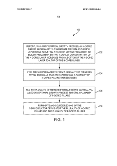
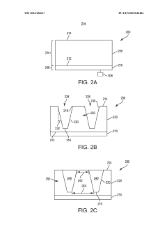
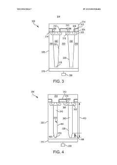
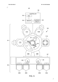
Gradient doping epitaxy in superjunction to improve breakdown voltage
PatentWO2023283417A1
Innovation
- A method involving epitaxial growth to form an n-doped layer with increasing dopant concentration from bottom to top, followed by etching to create tapered trenches and filling with p-doped material to form pillars, which helps in reducing voids and achieving charge balance between n and p regions.
Patent
Innovation
- Utilization of dopants to manipulate the effective nuclear charge in semiconductor materials, allowing precise control of band gap engineering without altering the crystal structure.
- Development of a quantitative model correlating effective nuclear charge adjustments with resulting band structure modifications, enabling predictive semiconductor design.
- Implementation of surface modification techniques that locally alter effective nuclear charge at interfaces, creating controlled band bending for improved device performance.
Quantum Effects in Nuclear Charge Modification
Quantum effects play a crucial role in the modification of effective nuclear charge in semiconductor materials, particularly at nanoscale dimensions where classical physics principles become insufficient. When semiconductor dimensions approach the de Broglie wavelength of charge carriers, quantum confinement effects emerge, fundamentally altering the electronic band structure and effective nuclear charge interactions.
The quantum mechanical treatment of nuclear charge modification reveals that electron wavefunctions experience significant perturbations when confined in low-dimensional semiconductor structures. This confinement leads to discrete energy levels rather than continuous bands, directly influencing how electrons experience the nuclear charge of constituent atoms. The quantization of energy states creates opportunities for precise manipulation of effective nuclear charge through quantum engineering approaches.
Quantum tunneling effects further complicate nuclear charge modification strategies by enabling electrons to penetrate potential barriers that would be insurmountable in classical physics. This tunneling phenomenon can be harnessed to modulate the effective nuclear charge experienced by carriers, particularly at heterojunction interfaces where band alignment creates quantum wells or barriers.
Many-body quantum effects, including electron-electron interactions and exchange-correlation phenomena, significantly impact the screening of nuclear charge in semiconductor materials. These quantum mechanical interactions can either enhance or diminish the effective nuclear charge experienced by carriers, depending on the specific material composition and structural configuration. Advanced computational methods such as density functional theory (DFT) with appropriate exchange-correlation functionals have become essential tools for accurately predicting these effects.
Quantum interference effects present another dimension for nuclear charge modification. When electron wave functions from different atomic sites overlap coherently, they can create interference patterns that modify the effective potential landscape experienced by charge carriers. This quantum interference can be engineered through precise atomic placement in semiconductor heterostructures or through the introduction of specific dopants at calculated positions.
Recent experimental advances in quantum metrology have enabled direct observation of these quantum effects on nuclear charge modification. Techniques such as scanning tunneling microscopy with atomic precision and angle-resolved photoemission spectroscopy (ARPES) now provide unprecedented insights into the quantum mechanical behavior of electrons in engineered semiconductor structures, validating theoretical models and enabling more precise band engineering approaches.
The exploitation of these quantum effects opens pathways to novel semiconductor devices with tailored electronic properties that transcend classical limitations, potentially revolutionizing next-generation electronics through quantum-engineered band structures.
Environmental Impact of Semiconductor Manufacturing Processes
The semiconductor manufacturing processes involved in band engineering through effective nuclear charge adjustment present significant environmental challenges. The manipulation of atomic structures at nanoscale requires extensive use of hazardous chemicals, including hydrofluoric acid, sulfuric acid, and various heavy metals that pose serious environmental risks when improperly managed.
Semiconductor fabrication facilities consume extraordinary amounts of water—up to millions of gallons daily for a single facility. The processes of doping, which directly relates to nuclear charge adjustment, often involve toxic elements such as arsenic, phosphorus, and boron. These dopants, when released into water systems, can cause long-term environmental contamination and health concerns in surrounding communities.
Energy consumption represents another critical environmental concern. The precise control of effective nuclear charge in semiconductor materials requires ultra-clean environments and highly controlled manufacturing conditions. Maintaining these cleanrooms demands enormous energy resources, contributing significantly to the carbon footprint of the semiconductor industry.
Waste management challenges are particularly acute in processes involving nuclear charge adjustment. The etching and cleaning steps generate substantial volumes of chemical waste containing perfluorocarbons (PFCs) and sulfur hexafluoride (SF6), which are potent greenhouse gases with global warming potentials thousands of times greater than carbon dioxide.
Recent technological advances have begun addressing these environmental impacts. Closed-loop water recycling systems have reduced freshwater consumption by up to 80% in some facilities. Alternative, less toxic materials are being explored for doping processes, including organic semiconductors that can achieve similar band engineering effects with reduced environmental impact.
Green chemistry principles are increasingly being applied to semiconductor manufacturing, with emphasis on atom economy and reduced use of hazardous substances. Some manufacturers have implemented abatement systems that can capture and neutralize over 90% of greenhouse gas emissions from fabrication processes.
Despite these improvements, the environmental footprint of semiconductor manufacturing remains substantial. As band engineering techniques become more sophisticated to meet demands for higher performance devices, the industry faces growing pressure to develop environmentally sustainable manufacturing approaches that maintain technological advancement while minimizing ecological harm.
Unlock deeper insights with Patsnap Eureka Quick Research — get a full tech report to explore trends and direct your research. Try now!
Generate Your Research Report Instantly with AI Agent
Supercharge your innovation with Patsnap Eureka AI Agent Platform!