

Enhancing Wafer Thinning for Semiconductor Yield Optimization
APR 7, 20269 MIN READ
Generate Your Research Report Instantly with AI Agent
PatSnap Eureka helps you evaluate technical feasibility & market potential.
Wafer Thinning Technology Background and Yield Goals
Wafer thinning technology emerged as a critical process in semiconductor manufacturing during the late 1980s when the industry began pursuing miniaturization and performance enhancement. Initially developed to reduce package thickness for portable electronics, this technology has evolved into a sophisticated process essential for advanced semiconductor devices. The fundamental principle involves mechanically and chemically reducing silicon wafer thickness from standard 725-775 micrometers to ultra-thin profiles ranging from 25 to 200 micrometers, depending on application requirements.
The evolution of wafer thinning has been driven by multiple technological demands including improved thermal management, reduced electrical resistance, enhanced signal integrity, and package miniaturization. Early implementations focused primarily on basic grinding techniques, but modern approaches integrate advanced chemical mechanical polishing, plasma etching, and stress relief processes. This progression reflects the semiconductor industry's continuous push toward higher performance density and more compact form factors.
Contemporary wafer thinning faces unprecedented challenges as device geometries shrink below 7 nanometers and three-dimensional architectures become mainstream. The technology must accommodate increasingly complex wafer structures including through-silicon vias, embedded components, and heterogeneous integration schemes. These developments have transformed wafer thinning from a relatively straightforward mechanical process into a precision engineering discipline requiring nanometer-level control and comprehensive process monitoring.
Current yield optimization goals center on achieving sub-micrometer thickness uniformity across entire wafer surfaces while maintaining structural integrity and electrical performance. Industry targets demand total thickness variation below 2 micrometers for 300mm wafers, with zero defect tolerance for critical applications such as image sensors and power semiconductors. Additionally, the process must preserve device functionality while enabling subsequent packaging operations including die attachment, wire bonding, and thermal interface material application.
The strategic importance of wafer thinning continues expanding as emerging applications in automotive electronics, 5G communications, and artificial intelligence processors demand enhanced thermal dissipation and electrical performance. Future developments must address challenges including ultra-thin wafer handling, stress-induced warpage control, and integration with advanced packaging technologies such as chiplet architectures and system-in-package solutions.
Market Demand for Advanced Semiconductor Thinning Solutions
The semiconductor industry is experiencing unprecedented demand for advanced wafer thinning solutions, driven by the relentless pursuit of miniaturization and performance enhancement across multiple technology sectors. Mobile devices, automotive electronics, and emerging applications such as artificial intelligence and Internet of Things devices require increasingly sophisticated semiconductor components that demand ultra-thin wafer processing capabilities.
Consumer electronics manufacturers are pushing for thinner, lighter devices with enhanced functionality, creating substantial market pressure for semiconductor companies to develop wafers with reduced thickness while maintaining structural integrity and electrical performance. The proliferation of 5G technology and edge computing applications has intensified this demand, as these technologies require high-performance chips in compact form factors.
The automotive sector represents a rapidly expanding market segment for advanced semiconductor thinning solutions. Electric vehicles and autonomous driving systems incorporate numerous sensors, processors, and power management chips that benefit from thin wafer technology. These applications demand exceptional reliability and thermal management capabilities, driving the need for precision thinning processes that can maintain consistent quality across large production volumes.
Data centers and cloud computing infrastructure are generating significant demand for high-density packaging solutions that rely heavily on advanced wafer thinning techniques. Server processors and memory devices require optimal thermal dissipation and space efficiency, making ultra-thin wafers essential for meeting performance and cost targets in these applications.
The market demand extends beyond traditional silicon-based semiconductors to compound semiconductor materials used in power electronics, radio frequency applications, and optoelectronics. These specialized materials present unique thinning challenges and opportunities, requiring tailored solutions that can handle different material properties while achieving the precision required for advanced packaging technologies.
Memory manufacturers are particularly driving demand for advanced thinning solutions as they pursue three-dimensional NAND flash architectures and high-bandwidth memory configurations. These applications require extremely uniform thickness control and minimal surface damage to ensure optimal electrical performance and manufacturing yield.
The growing adoption of system-in-package and wafer-level packaging technologies is creating additional market opportunities for sophisticated thinning equipment and processes. These packaging approaches enable higher integration density and improved electrical performance, but they require precise control over wafer thickness variations and surface quality parameters that challenge conventional thinning methods.
Current Wafer Thinning Challenges and Process Limitations
Wafer thinning processes face significant challenges in achieving uniform thickness distribution across large-diameter wafers. Current grinding and polishing techniques struggle to maintain consistent material removal rates, particularly at wafer edges where stress concentrations and thermal effects create non-uniform processing conditions. This variability directly impacts device performance and yield, as thickness variations can lead to electrical parameter deviations and mechanical stress-induced defects.
Subsurface damage represents a critical limitation in conventional mechanical thinning approaches. Diamond grinding wheels and abrasive slurries generate microcracks and crystal lattice disruptions that extend several micrometers below the processed surface. These defects compromise device reliability and require extensive damage removal steps, increasing processing time and material waste while potentially introducing additional surface irregularities.
Thermal management during high-speed grinding operations poses substantial technical constraints. Heat generation from mechanical friction can cause wafer warpage, induce thermal stress, and alter material properties in sensitive device regions. Current cooling systems often provide inadequate temperature control, leading to process instabilities and requiring conservative processing parameters that limit throughput and efficiency.
Process control and metrology limitations hinder real-time optimization of thinning operations. Existing thickness measurement systems lack the spatial resolution and speed necessary for closed-loop process control during high-volume manufacturing. This results in reactive rather than predictive process adjustments, contributing to yield losses and increased scrap rates.
Chemical mechanical planarization integration challenges emerge when combining thinning with subsequent processing steps. Current CMP slurries and pad technologies are not optimized for ultra-thin wafer handling, leading to increased breakage rates and surface contamination issues. The transition between mechanical thinning and chemical polishing often creates interface defects that propagate through final device structures.
Wafer handling and support mechanisms represent fundamental process limitations. Conventional vacuum chucks and carrier systems induce mechanical stress that can cause wafer cracking or deformation during thinning operations. These handling constraints become increasingly critical as target thicknesses decrease below 50 micrometers, where mechanical fragility significantly impacts process yield and reliability.
Existing Wafer Thinning Process Solutions
01 Wafer grinding and polishing process optimization
Optimizing the grinding and polishing processes is crucial for improving wafer thinning yield. This includes controlling grinding parameters such as pressure, speed, and abrasive selection to minimize surface damage and subsurface defects. Advanced polishing techniques can reduce micro-cracks and improve surface quality, leading to higher yield rates in thinned wafers. Process monitoring and real-time adjustments help maintain consistent quality throughout the thinning operation.- Wafer grinding and polishing process optimization: Optimizing the grinding and polishing processes is crucial for improving wafer thinning yield. This involves controlling grinding parameters such as pressure, speed, and abrasive selection to minimize surface damage and subsurface defects. Advanced polishing techniques can reduce micro-cracks and improve surface quality, leading to higher yield rates. Process monitoring and real-time feedback systems help maintain consistent quality throughout the thinning operation.
- Wafer handling and support systems: Proper wafer handling and support mechanisms are essential to prevent breakage during thinning operations. This includes the use of specialized chuck systems, vacuum holders, and protective tapes that provide adequate support while allowing uniform material removal. Improved handling systems reduce stress concentration points and minimize edge chipping. Advanced mounting techniques ensure stable fixation throughout the thinning process, significantly improving yield.
- Stress management and wafer strengthening: Managing internal stress and strengthening wafer structures are key factors in improving thinning yield. Techniques include stress relief annealing, application of reinforcement layers, and controlled cooling processes. These methods help prevent warping, cracking, and breakage during and after thinning. Stress distribution analysis and compensation strategies enable the production of ultra-thin wafers with improved mechanical stability and higher survival rates.
- Defect detection and quality control: Implementing advanced defect detection and quality control systems is critical for maximizing wafer thinning yield. This involves in-line inspection technologies, automated optical inspection, and non-destructive testing methods to identify defects early in the process. Real-time monitoring allows for immediate process adjustments to prevent defect propagation. Statistical process control and yield prediction models help optimize parameters and reduce scrap rates.
- Multi-step thinning and back-grinding techniques: Employing multi-step thinning strategies and optimized back-grinding techniques enhances yield by gradually reducing wafer thickness in controlled stages. This approach minimizes mechanical shock and thermal stress on the wafer. Sequential grinding with progressively finer abrasives reduces subsurface damage and improves final surface quality. Combination methods integrating chemical-mechanical processes with mechanical grinding achieve superior results with higher throughput and yield.
02 Wafer handling and support systems
Proper wafer handling and support mechanisms are essential to prevent breakage during the thinning process. This includes the use of temporary bonding materials, carrier wafers, and specialized chuck designs that provide uniform support across the wafer surface. Advanced handling systems reduce stress concentration points and minimize the risk of wafer cracking or chipping during grinding and subsequent processing steps. These support systems are particularly important for ultra-thin wafer applications.Expand Specific Solutions03 Stress management and defect reduction
Managing internal stress and reducing defects in thinned wafers significantly impacts yield. Techniques include stress relief treatments, controlled cooling processes, and the use of protective layers to prevent crack propagation. Understanding the relationship between wafer thickness, material properties, and stress distribution helps in developing processes that minimize warpage and breakage. Detection and mitigation of defects such as micro-cracks, scratches, and edge chipping are critical for maintaining high yield rates.Expand Specific Solutions04 Advanced thinning equipment and automation
Modern thinning equipment with advanced automation capabilities improves yield through precise control and monitoring. This includes automated grinding systems with in-situ thickness measurement, adaptive process control, and defect detection systems. Equipment design features such as improved spindle stability, uniform pressure distribution, and contamination control contribute to higher yield rates. Integration of sensors and feedback mechanisms enables real-time process optimization and reduces human error.Expand Specific Solutions05 Quality inspection and yield monitoring methods
Comprehensive quality inspection and yield monitoring systems are essential for identifying and addressing yield-limiting factors in wafer thinning. This includes non-destructive testing methods, statistical process control, and defect classification systems. Advanced inspection techniques can detect subsurface damage, thickness variations, and other quality issues that affect yield. Data analysis and yield modeling help identify process improvements and predict potential failure modes, enabling proactive adjustments to maintain high yield rates.Expand Specific Solutions
Key Players in Wafer Thinning Equipment and Services
The wafer thinning semiconductor market represents a mature yet rapidly evolving competitive landscape driven by increasing demand for miniaturized, high-performance devices. The industry is in an advanced growth stage with significant market expansion fueled by 5G, automotive electronics, and IoT applications. Technology maturity varies significantly across players, with established foundries like Taiwan Semiconductor Manufacturing Co. and Samsung Electronics leading in advanced process capabilities and ultra-thin wafer technologies. Memory specialists including Micron Technology and Yangtze Memory Technologies demonstrate sophisticated thinning expertise for 3D NAND applications. Equipment manufacturers such as Tokyo Seimitsu and specialized firms like SILTECTRA provide critical enabling technologies. Chinese players including Semiconductor Manufacturing International and Shanghai Huali are rapidly advancing their capabilities, while traditional leaders like Intel and GlobalFoundries maintain strong positions through continuous innovation in substrate engineering and yield optimization techniques.
Taiwan Semiconductor Manufacturing Co., Ltd.
Technical Solution: TSMC employs advanced wafer thinning technologies including backside grinding, chemical mechanical polishing (CMP), and plasma etching processes. Their approach integrates precision grinding wheels with diamond abrasives to achieve wafer thickness down to 25-50 micrometers for advanced packaging applications. The company utilizes multi-step thinning processes with stress relief annealing to minimize wafer warpage and maintain structural integrity. TSMC's wafer thinning capability supports their advanced packaging technologies including InFO (Integrated Fan-Out) and CoWoS (Chip on Wafer on Substrate) platforms, enabling higher device density and improved thermal performance for mobile and high-performance computing applications.
Strengths: Industry-leading precision control and yield rates, extensive experience with advanced node processing. Weaknesses: High capital investment requirements, complex process integration challenges.
Tokyo Seimitsu Co., Ltd.
Technical Solution: Tokyo Seimitsu provides comprehensive wafer thinning equipment solutions including precision grinding systems, polishing equipment, and measurement tools. Their DFG (Dual Feed Grinder) series offers high-precision wafer thinning capabilities with thickness uniformity control within ±0.5 micrometers across 300mm wafers. The company's systems integrate advanced spindle technology, precision chuck mechanisms, and real-time monitoring systems to optimize grinding processes. Tokyo Seimitsu's equipment supports various thinning applications from thick wafer processing to ultra-thin wafer handling for advanced packaging. Their solutions include automated handling systems, contamination control features, and process optimization software to enhance yield and productivity in semiconductor manufacturing environments.
Strengths: Leading equipment technology and precision control systems, comprehensive automation solutions. Weaknesses: Equipment supplier rather than process developer, dependent on customer process optimization expertise.
Core Innovations in Advanced Thinning Techniques
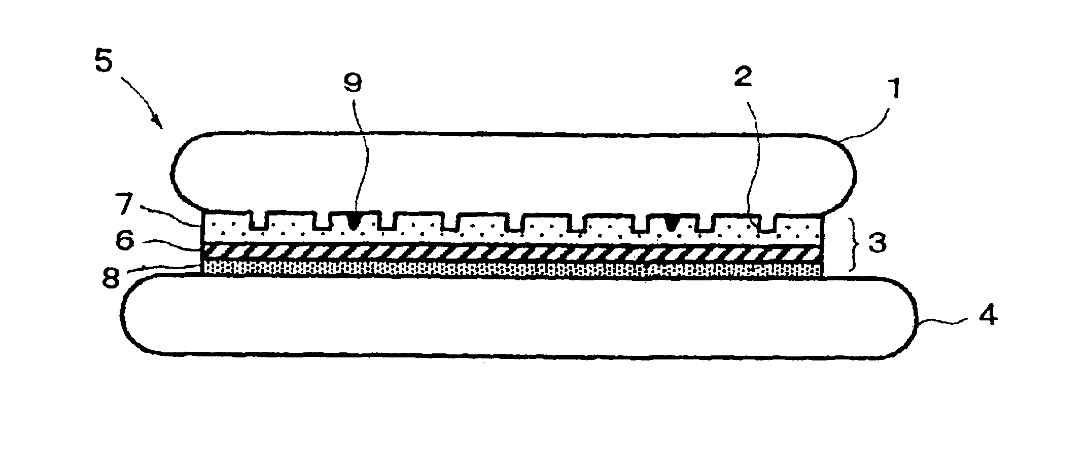
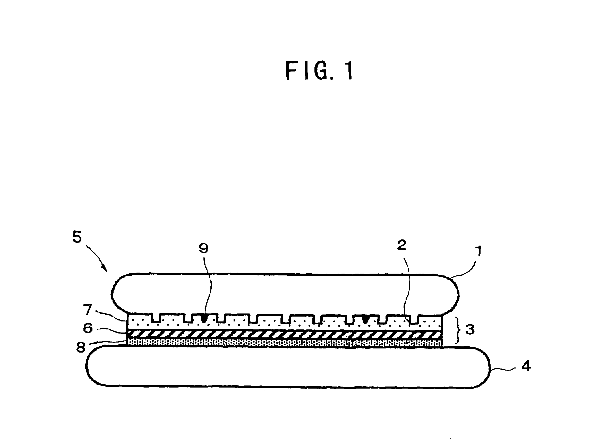
Semiconductor wafer thinning method, and thin semiconductor wafer
PatentInactiveUS6930023B2
Innovation
- A method involving adhering the semiconductor wafer to a support via an adhesive layer, specifically a thermal release double-sided adhesive sheet, and grinding the back surface to achieve thinner wafers without breakage, allowing for easy release and minimizing stress through matching thermal expansion coefficients and using a larger adhesive surface for secure adhesion.

Semiconductor wafer and method of wafer thinning
PatentPendingUS20250062114A1
Innovation
- A method involving a grinding phase followed by a separation phase, where the grinding wheel lifts off the surface and rinsing solution is used to clear particles and contaminants, reducing surface damage and improving the final surface quality.


Environmental Impact of Wafer Thinning Processes
The environmental implications of wafer thinning processes have become increasingly significant as semiconductor manufacturing scales up to meet global demand. Traditional mechanical grinding and chemical-mechanical polishing methods generate substantial waste streams, including silicon particulates, chemical slurries, and contaminated process fluids. These byproducts require specialized treatment and disposal protocols, contributing to the overall environmental footprint of semiconductor fabrication facilities.
Chemical etching processes, while offering superior surface quality, introduce additional environmental concerns through the use of hazardous chemicals such as hydrofluoric acid, potassium hydroxide, and various organic solvents. The atmospheric emissions from these processes include volatile organic compounds and acid vapors that necessitate sophisticated scrubbing systems and air quality monitoring. Water consumption for cleaning and rinsing operations further amplifies the environmental impact, particularly in regions facing water scarcity challenges.
Energy consumption represents another critical environmental factor, as wafer thinning equipment requires substantial electrical power for vacuum systems, heating elements, and precision control mechanisms. Advanced plasma-based thinning processes, while offering improved precision, typically consume 20-30% more energy compared to conventional mechanical methods. The carbon footprint associated with this energy usage varies significantly depending on regional power generation sources and facility efficiency measures.
Waste heat generation from thinning processes contributes to facility cooling requirements, creating additional energy demands and potential thermal pollution concerns. Modern semiconductor fabs are implementing heat recovery systems to capture and repurpose waste thermal energy, though adoption rates remain limited due to infrastructure costs and technical complexity.
Emerging sustainable approaches focus on process optimization to minimize material waste, closed-loop chemical recycling systems, and the development of environmentally benign thinning chemistries. Industry initiatives are exploring plasma-free alternatives and bio-based processing aids to reduce the environmental burden while maintaining production efficiency and yield requirements.
Quality Control Standards for Thinned Wafer Manufacturing
Quality control standards for thinned wafer manufacturing represent a critical framework ensuring consistent product quality and manufacturing reliability in semiconductor production. These standards encompass comprehensive measurement protocols, defect detection methodologies, and acceptance criteria that govern the entire thinning process from initial substrate preparation through final inspection.
Thickness uniformity standards constitute the primary quality metric, typically requiring total thickness variation (TTV) within ±2-5 micrometers across the wafer surface. Advanced metrology systems employ capacitive sensors, optical interferometry, and contact profilometry to achieve measurement accuracies of ±0.1 micrometers. Statistical process control charts monitor thickness distribution patterns, enabling real-time process adjustments and trend analysis.
Surface quality specifications address critical parameters including surface roughness, micro-scratches, and contamination levels. Root mean square (RMS) roughness values must typically remain below 1-2 nanometers for optimal device performance. Automated optical inspection systems utilize high-resolution cameras and laser scanning to detect surface anomalies, while particle counters monitor contamination levels according to cleanroom classification standards.
Mechanical integrity assessments evaluate wafer strength and stress distribution through non-destructive testing methods. Bow and warp measurements ensure dimensional stability within specified tolerances, typically less than 50 micrometers for 300mm wafers. Stress mapping techniques identify potential failure points and optimize handling procedures to minimize breakage risks during subsequent processing steps.
Edge quality control addresses chipping, edge roll-off, and exclusion zone specifications that directly impact die yield at wafer peripheries. Precision edge profiling systems measure bevel angles and edge geometry to ensure compatibility with downstream packaging processes. Standardized edge preparation protocols minimize stress concentrations that could propagate into active device areas.
Documentation and traceability requirements establish comprehensive quality records linking process parameters to final product characteristics. Statistical sampling plans balance inspection thoroughness with production efficiency, while automated data collection systems enable rapid quality trend identification and corrective action implementation across multiple production lots.
Unlock deeper insights with PatSnap Eureka Quick Research — get a full tech report to explore trends and direct your research. Try now!
Generate Your Research Report Instantly with AI Agent
Supercharge your innovation with PatSnap Eureka AI Agent Platform!