

EUV Lithography for High-Density Plasmonics: Feasibility Study
APR 2, 20269 MIN READ
Generate Your Research Report Instantly with AI Agent
Patsnap Eureka helps you evaluate technical feasibility & market potential.
EUV Lithography Plasmonics Background and Objectives
Extreme Ultraviolet (EUV) lithography represents a revolutionary advancement in semiconductor manufacturing, utilizing 13.5 nm wavelength radiation to achieve unprecedented pattern resolution capabilities. This technology has emerged as the cornerstone for producing sub-10 nm semiconductor devices, enabling the continuation of Moore's Law in an era where traditional optical lithography approaches physical limitations.
The intersection of EUV lithography with plasmonics opens new frontiers in nanofabrication, particularly for high-density plasmonic structures that require feature sizes well below 100 nanometers. Plasmonics, which exploits the interaction between electromagnetic fields and free electrons in metals, demands precise control over nanoscale geometries to achieve desired optical properties and field enhancement effects.
Traditional lithographic techniques, including deep ultraviolet (DUV) lithography at 193 nm wavelength, face significant challenges when fabricating plasmonic nanostructures with the required precision and density. Multiple patterning techniques and complex resist processing often introduce variability and limit the achievable structure density, compromising plasmonic device performance.
The primary objective of this feasibility study centers on evaluating EUV lithography's capability to fabricate high-density plasmonic nanostructures with enhanced precision and reduced manufacturing complexity. Key technical goals include achieving sub-20 nm feature resolution for plasmonic elements, maintaining critical dimension uniformity across large substrate areas, and enabling direct single-exposure patterning of complex plasmonic arrays.
Secondary objectives encompass assessing the compatibility of EUV processes with plasmonic material systems, including noble metals and alternative plasmonic materials. The study aims to determine optimal resist formulations and processing conditions that preserve the optical properties of plasmonic structures while achieving the required dimensional accuracy.
Economic and scalability considerations form additional objectives, focusing on evaluating the cost-effectiveness of EUV-based plasmonic device manufacturing compared to existing multi-step fabrication approaches. The investigation seeks to establish whether EUV lithography can provide a viable pathway for mass production of high-performance plasmonic devices across applications ranging from optical sensing to quantum photonics.
Market Demand for High-Density Plasmonic Devices
The market demand for high-density plasmonic devices is experiencing unprecedented growth driven by the convergence of multiple technological trends and application requirements. The telecommunications industry represents the largest demand driver, particularly with the global deployment of 5G networks and the emerging development of 6G technologies. These next-generation communication systems require advanced optical components capable of handling massive data throughput while maintaining compact form factors, creating substantial opportunities for plasmonic devices that can manipulate light at subwavelength scales.
Consumer electronics markets are increasingly demanding miniaturized optical components for applications ranging from advanced smartphone cameras to augmented reality displays. The push toward thinner, lighter devices with enhanced optical capabilities has created a significant market pull for high-density plasmonic solutions that can replace traditional bulky optical elements. Major consumer electronics manufacturers are actively seeking plasmonic technologies to enable new functionalities while reducing device footprint.
The healthcare and biotechnology sectors represent rapidly expanding markets for plasmonic devices, particularly in biosensing and medical diagnostics applications. The ability of plasmonic structures to enhance electromagnetic fields at nanoscale dimensions makes them ideal for detecting minute biological changes, driving demand from point-of-care diagnostic device manufacturers and laboratory equipment providers.
Data center and cloud computing infrastructure development is creating substantial demand for high-performance optical interconnects and photonic integrated circuits. As data processing requirements continue to escalate, traditional electronic solutions face fundamental limitations, necessitating the adoption of plasmonic technologies for efficient light-matter interaction at chip scale.
The automotive industry's transition toward autonomous vehicles and advanced driver assistance systems is generating new demand for compact, high-performance optical sensors and communication devices. Plasmonic technologies offer potential solutions for LiDAR systems, optical communication between vehicles, and advanced sensing applications required for autonomous navigation.
Emerging applications in quantum computing and quantum communication are creating niche but high-value market segments for specialized plasmonic devices. These applications require precise control over light-matter interactions at quantum scales, representing a premium market opportunity for advanced plasmonic solutions.
The overall market trajectory indicates strong growth potential across multiple sectors, with increasing recognition of plasmonic technologies as enabling solutions for next-generation optical and optoelectronic applications requiring unprecedented levels of miniaturization and performance.
Current EUV Lithography Challenges for Plasmonic Structures
EUV lithography faces significant technical barriers when applied to fabricating high-density plasmonic structures, primarily due to the fundamental mismatch between current system capabilities and the stringent requirements of plasmonic devices. The most critical challenge lies in achieving the sub-10 nanometer feature sizes essential for effective plasmonic resonance while maintaining the precise geometric control necessary for optimal optical performance.
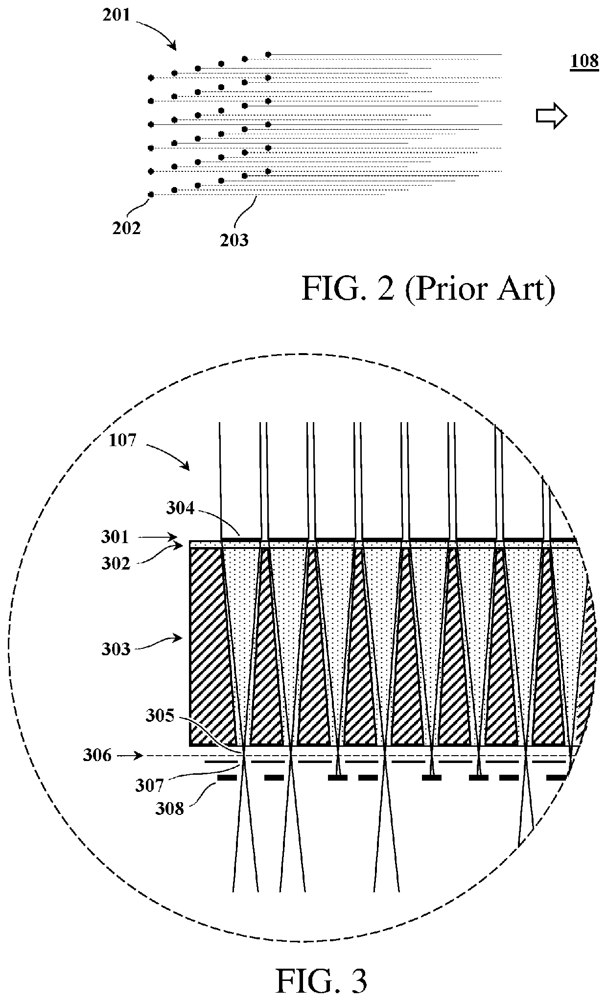
Resolution limitations represent a primary constraint, as current EUV systems typically achieve 13-7 nanometer half-pitch resolution under optimal conditions. However, plasmonic structures often require feature dimensions below 5 nanometers to achieve desired optical properties, particularly for applications in the visible and near-infrared spectrum. This resolution gap becomes more pronounced when considering the need for complex three-dimensional geometries that characterize advanced plasmonic devices.
Line edge roughness (LER) and line width roughness (LWR) pose particularly severe challenges for plasmonic applications. While semiconductor devices can tolerate roughness values of 2-3 nanometers, plasmonic structures require surface smoothness approaching atomic scales to minimize scattering losses and maintain coherent electromagnetic field enhancement. Current EUV processes struggle to achieve the sub-nanometer roughness levels demanded by high-performance plasmonic devices.
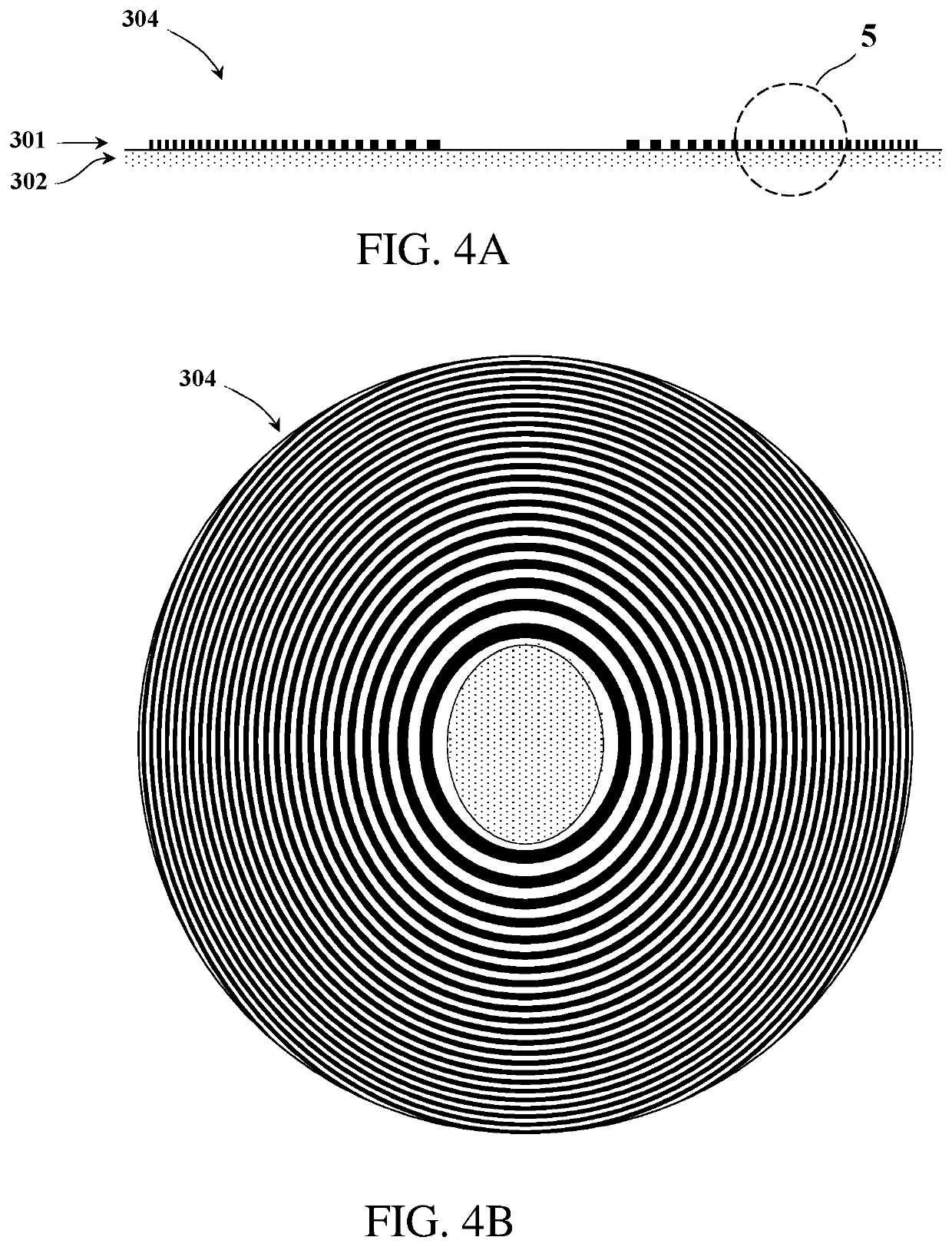
Pattern fidelity issues emerge when attempting to fabricate the intricate geometries typical of plasmonic structures, such as split-ring resonators, bow-tie antennas, and complex metamaterial arrays. EUV lithography exhibits systematic pattern distortions and corner rounding effects that significantly impact the electromagnetic response of these structures, where even minor geometric deviations can shift resonance frequencies and reduce field enhancement factors.
Resist chemistry limitations further complicate plasmonic structure fabrication. Current EUV resists are optimized for semiconductor manufacturing requirements rather than the unique demands of plasmonic devices. The chemical composition and molecular structure of existing resists can interfere with subsequent metallization processes essential for plasmonic functionality, leading to adhesion problems and interface contamination.
Throughput constraints become particularly problematic for plasmonic applications requiring large-area patterning or high-volume manufacturing. The inherently low photon flux of EUV sources, combined with the extended exposure times needed for high-resolution plasmonic features, results in economically challenging processing speeds that may limit commercial viability for many plasmonic device applications.
Resolution limitations represent a primary constraint, as current EUV systems typically achieve 13-7 nanometer half-pitch resolution under optimal conditions. However, plasmonic structures often require feature dimensions below 5 nanometers to achieve desired optical properties, particularly for applications in the visible and near-infrared spectrum. This resolution gap becomes more pronounced when considering the need for complex three-dimensional geometries that characterize advanced plasmonic devices.
Line edge roughness (LER) and line width roughness (LWR) pose particularly severe challenges for plasmonic applications. While semiconductor devices can tolerate roughness values of 2-3 nanometers, plasmonic structures require surface smoothness approaching atomic scales to minimize scattering losses and maintain coherent electromagnetic field enhancement. Current EUV processes struggle to achieve the sub-nanometer roughness levels demanded by high-performance plasmonic devices.
Pattern fidelity issues emerge when attempting to fabricate the intricate geometries typical of plasmonic structures, such as split-ring resonators, bow-tie antennas, and complex metamaterial arrays. EUV lithography exhibits systematic pattern distortions and corner rounding effects that significantly impact the electromagnetic response of these structures, where even minor geometric deviations can shift resonance frequencies and reduce field enhancement factors.
Resist chemistry limitations further complicate plasmonic structure fabrication. Current EUV resists are optimized for semiconductor manufacturing requirements rather than the unique demands of plasmonic devices. The chemical composition and molecular structure of existing resists can interfere with subsequent metallization processes essential for plasmonic functionality, leading to adhesion problems and interface contamination.
Throughput constraints become particularly problematic for plasmonic applications requiring large-area patterning or high-volume manufacturing. The inherently low photon flux of EUV sources, combined with the extended exposure times needed for high-resolution plasmonic features, results in economically challenging processing speeds that may limit commercial viability for many plasmonic device applications.
Existing EUV Solutions for Plasmonic Device Fabrication
01 EUV light source and collector optimization for high-density patterning
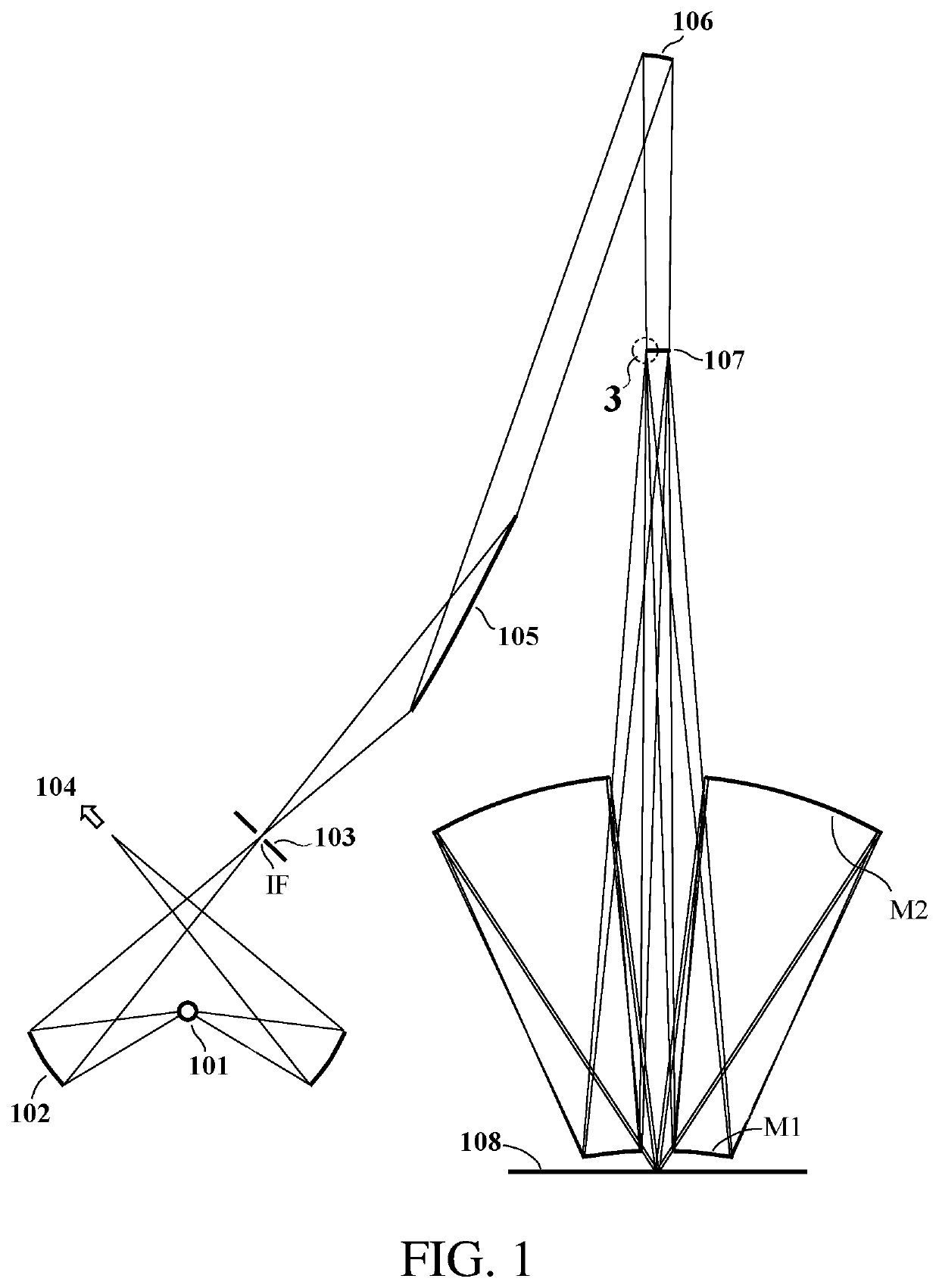
Extreme ultraviolet lithography systems require optimized light sources and collector optics to achieve high-density pattern transfer. The light source generates EUV radiation at specific wavelengths, typically around 13.5 nm, while collector mirrors with specialized multilayer coatings efficiently gather and direct the radiation toward the illumination optics. Advanced collector designs incorporate ellipsoidal or other aspherical geometries to maximize collection efficiency and minimize radiation loss, enabling the high photon flux necessary for high-resolution, high-density semiconductor manufacturing.- EUV light source and collector optimization for high-density patterning: Extreme ultraviolet lithography systems require optimized light sources and collector optics to achieve high-density pattern transfer. The light source generates EUV radiation at specific wavelengths, typically around 13.5 nm, which is then collected and directed toward the mask using specialized multilayer mirrors. Collector design focuses on maximizing light collection efficiency while minimizing debris contamination. Advanced collector geometries and coatings enable higher power delivery to the wafer, supporting smaller feature sizes and increased pattern density in semiconductor manufacturing.
- EUV mask and pellicle technology for defect-free high-density imaging: High-density EUV lithography requires advanced mask structures and protective pellicles to prevent defects during exposure. Masks utilize reflective multilayer coatings optimized for EUV wavelengths, with absorber patterns defining the circuit features. Pellicle membranes protect masks from particle contamination while maintaining high EUV transmission. The mask infrastructure includes specialized materials and fabrication processes that ensure pattern fidelity at nanometer scales, enabling the production of high-density integrated circuits with minimal defects.
- High numerical aperture projection optics for enhanced resolution: Achieving high-density patterns in EUV lithography requires projection optics with high numerical aperture values. The optical system consists of multiple reflective mirrors arranged to focus EUV light onto the wafer with minimal aberrations. Advanced mirror designs, including aspherical surfaces and optimized multilayer coatings, enable resolution enhancement necessary for sub-10nm feature sizes. The projection system architecture balances throughput, resolution, and depth of focus to support high-density semiconductor manufacturing requirements.
- EUV resist materials and processing for high-density pattern formation: Specialized photoresist materials are essential for high-density EUV lithography applications. These resists must exhibit high sensitivity to EUV radiation while maintaining excellent resolution and low line edge roughness. Chemical formulations include photoacid generators, polymers, and additives optimized for EUV exposure wavelengths. Processing techniques involve precise coating, exposure, and development steps that enable pattern transfer at nanometer dimensions. Advanced resist platforms support the creation of high-density circuit patterns with improved process windows.
- Multi-patterning and computational lithography techniques for density enhancement: High-density pattern formation in EUV lithography is enhanced through multi-patterning strategies and computational lithography methods. These approaches decompose complex patterns into multiple exposure steps or utilize advanced algorithms to optimize mask designs. Computational techniques include optical proximity correction, source-mask optimization, and inverse lithography technology. Multi-patterning methods enable pitch division and pattern density multiplication beyond single-exposure limits. Combined with EUV technology, these techniques achieve the ultra-high pattern densities required for advanced semiconductor nodes.
02 Photoresist materials and processes for EUV high-density lithography
Specialized photoresist materials are essential for achieving high-density patterns in EUV lithography. These materials must exhibit high sensitivity to EUV radiation while maintaining excellent resolution and low line edge roughness. Chemical amplification mechanisms and novel polymer compositions enable the required sensitivity, while controlled molecular weight distributions and optimized formulations reduce defects. Post-exposure processing techniques, including specific baking temperatures and development conditions, further enhance pattern fidelity and enable the creation of ultra-fine features necessary for high-density integrated circuits.Expand Specific Solutions03 Mask and reticle technologies for high-density EUV patterning
EUV masks and reticles employ reflective multilayer structures rather than traditional transmissive designs to accommodate the short wavelength of EUV radiation. These masks consist of alternating layers of materials with different refractive indices, typically molybdenum and silicon, deposited on ultra-flat substrates. Absorber patterns define the circuit features, and advanced mask architectures incorporate phase-shifting elements and optimized absorber materials to enhance contrast and enable high-density pattern transfer. Defect mitigation strategies and inspection techniques ensure mask quality for high-volume manufacturing.Expand Specific Solutions04 Optical system design and projection optics for high-density imaging
The projection optical system in EUV lithography tools utilizes all-reflective designs with multiple aspherical mirrors to achieve the numerical aperture and resolution required for high-density patterning. These systems employ sophisticated mirror arrangements, typically consisting of four to six mirrors with precise surface figures and multilayer coatings optimized for EUV wavelengths. Aberration correction techniques, including mirror positioning adjustments and wavefront control, maintain imaging quality across the exposure field. Advanced illumination schemes and pupil filtering methods further enhance resolution and depth of focus for dense pattern features.Expand Specific Solutions05 Contamination control and vacuum systems for EUV high-density manufacturing
EUV lithography requires ultra-high vacuum environments and stringent contamination control to prevent absorption of EUV radiation and maintain optical performance. Vacuum systems maintain pressures below specified thresholds to minimize radiation attenuation by residual gases. Contamination mitigation strategies include protective gas flows, in-situ cleaning processes, and specialized materials that resist carbon deposition and oxidation. Particle control measures and environmental monitoring systems ensure that optical surfaces remain clean throughout extended operation, enabling consistent high-density pattern transfer and maximizing system uptime in production environments.Expand Specific Solutions
Key Players in EUV Lithography and Plasmonics Industry
The EUV lithography for high-density plasmonics field represents a mature yet rapidly evolving technology sector within the advanced semiconductor manufacturing industry. The market demonstrates significant scale with established players like ASML Netherlands BV dominating EUV lithography systems, while Taiwan Semiconductor Manufacturing Co., Samsung Electronics, and Intel Corp. drive demand through cutting-edge chip production. Technology maturity varies across the ecosystem, with ASML achieving commercial EUV deployment while companies like Cymer LLC, Nikon Corp., and Tokyo Electron Ltd. continue advancing complementary technologies. Applied Materials and NuFlare Technology contribute specialized equipment solutions, while material suppliers including Shanghai Sinyang Semiconductor and AGC Inc. develop critical photoresists and optical components. The competitive landscape shows consolidation around proven EUV capabilities, though emerging applications in plasmonics create opportunities for innovation among research institutions like Princeton University and specialized technology developers.
Taiwan Semiconductor Manufacturing Co., Ltd.
Technical Solution: TSMC has successfully implemented EUV lithography in their advanced process nodes including 7nm, 5nm, and 3nm technologies, demonstrating feasibility for high-density plasmonic device fabrication. Their EUV-enabled processes achieve critical dimensions below 10nm with excellent uniformity across 300mm wafers. TSMC's approach combines EUV lithography with advanced materials and process optimization to create plasmonic structures with precise geometric control. They have developed specialized design rules and manufacturing flows that leverage EUV's single-patterning capability to reduce process complexity while maintaining the tight tolerances required for plasmonic applications.
Strengths: Proven high-volume EUV manufacturing experience with excellent yield and process stability for nanoscale structures. Weaknesses: Limited flexibility for custom plasmonic designs due to standardized manufacturing processes and high minimum order quantities.
Intel Corp.
Technical Solution: Intel has extensively researched EUV lithography applications for advanced semiconductor manufacturing and has explored its potential for plasmonic device fabrication. Their approach focuses on leveraging EUV's single-exposure capability to create complex plasmonic nanostructures without multiple patterning steps. Intel's research demonstrates EUV feasibility for creating high-density plasmonic arrays with feature sizes down to 7nm and pitch scaling suitable for optical applications. They have developed specialized resist materials and process conditions optimized for plasmonic structure formation, including metal deposition and etching techniques that preserve the critical dimensions achieved through EUV patterning.
Strengths: Strong R&D capabilities in EUV process development and extensive experience with nanoscale manufacturing processes. Weaknesses: Primary focus on logic devices rather than specialized plasmonic applications, limiting dedicated development resources for this specific field.
Core EUV Innovations for High-Density Plasmonics
Organotin cluster photoresists and stabilization methods
PatentPendingUS20240353752A1
Innovation
- The use of organic molecules with functional groups such as —SH, —OH, —NH2, —COOH, and others to stabilize organotin clusters, preventing aggregation and precipitation, and improving solubility, thereby enhancing the stability, shelf life, and uniformity of the photoresists for EUV lithography.


EUV Lithography System with Diffraction Optics
PatentActiveUS20220107568A1
Innovation
- A new EUV maskless lithography design using an array of simple binary-optic zone-plate microlenses that focus EUV illumination onto a writing surface, with diffractive projection mirrors to neutralize chromatic and geometric aberrations, allowing for higher optical efficiency and the potential to operate at reduced wavelengths, and transforming the microlens array into a holographic transmission mask for full-field image formation.

EUV Equipment Export Control and Trade Regulations
The global trade landscape for EUV lithography equipment is governed by a complex web of export control regulations that significantly impact the development and deployment of advanced semiconductor manufacturing technologies. The Wassenaar Arrangement serves as the primary multilateral framework, establishing dual-use technology controls that classify EUV systems as strategically sensitive equipment requiring export licenses. These regulations directly affect the feasibility of implementing EUV lithography for high-density plasmonic applications, as access to cutting-edge equipment remains restricted to specific jurisdictions and end-users.
The United States maintains the most stringent export control regime through the Export Administration Regulations (EAR), which classify EUV lithography systems under Category 3 of the Commerce Control List. The Bureau of Industry and Security requires comprehensive end-user verification and imposes strict licensing requirements for EUV equipment exports to certain countries. These controls extend beyond complete systems to include critical components, software, and technical data necessary for EUV operations, creating substantial barriers for international research collaborations in plasmonic device fabrication.
European Union export controls, implemented through the Dual-Use Regulation, align closely with Wassenaar guidelines while maintaining some flexibility for intra-EU transfers. ASML, the dominant EUV equipment manufacturer, operates under Dutch export licensing requirements that have become increasingly restrictive. The Netherlands has implemented additional national controls beyond EU requirements, particularly affecting shipments to Asia-Pacific regions where significant plasmonic research activities are concentrated.
Recent geopolitical tensions have intensified export control enforcement, with new restrictions targeting specific countries and entities involved in advanced semiconductor research. The CHIPS and Science Act in the United States has introduced additional compliance requirements for recipients of federal funding, potentially limiting international partnerships in EUV-based plasmonic research. These evolving regulations create uncertainty for long-term research planning and technology transfer agreements.
The regulatory environment poses particular challenges for academic institutions and research organizations pursuing EUV lithography applications in plasmonics. Deemed export regulations restrict the sharing of technical knowledge with foreign nationals, complicating international research collaborations. Additionally, the high cost of compliance and licensing procedures may limit access to EUV technology for specialized applications like plasmonic device fabrication, where commercial volumes are typically lower than mainstream semiconductor production.
Environmental Impact of EUV Lithography Processes
EUV lithography processes present significant environmental challenges that require comprehensive assessment and mitigation strategies. The technology's environmental footprint stems primarily from its extraordinary energy consumption, with EUV scanners requiring approximately 10-20 times more electrical power than conventional deep ultraviolet systems. This elevated energy demand translates to substantial carbon emissions, particularly in regions where electricity generation relies heavily on fossil fuels.
The generation of EUV radiation through laser-produced plasma or discharge-produced plasma mechanisms necessitates continuous operation of high-power laser systems, typically consuming 200-400 kW of electrical power. Additionally, the extensive cooling infrastructure required to maintain optimal operating temperatures for critical components further amplifies energy consumption. The environmental impact is compounded by the need for specialized cleanroom facilities with enhanced contamination control systems.
Chemical waste generation represents another critical environmental concern in EUV lithography operations. The process requires specialized photoresists and cleaning solvents that often contain fluorinated compounds and other environmentally persistent substances. These materials demand careful handling, treatment, and disposal protocols to prevent environmental contamination. The tin debris generated in laser-produced plasma EUV sources creates additional waste streams requiring specialized management procedures.
Water consumption for cooling systems and facility operations constitutes a substantial environmental burden, particularly in semiconductor manufacturing regions facing water scarcity. EUV facilities typically require continuous water circulation systems for temperature regulation, leading to significant consumption rates and potential thermal pollution of water bodies.
The manufacturing and maintenance of EUV systems involve rare earth elements and specialized materials with complex supply chains and associated environmental impacts. Component replacement cycles, while improving with technological advancement, still generate electronic waste requiring proper recycling protocols.
Emerging mitigation strategies include implementation of renewable energy sources, development of more efficient EUV source technologies, and advancement in waste treatment processes. Industry initiatives focus on establishing circular economy principles within EUV manufacturing ecosystems, emphasizing material recovery and process optimization to minimize environmental impact while maintaining the precision required for high-density plasmonic device fabrication.
Unlock deeper insights with Patsnap Eureka Quick Research — get a full tech report to explore trends and direct your research. Try now!
Generate Your Research Report Instantly with AI Agent
Supercharge your innovation with Patsnap Eureka AI Agent Platform!