

How to Mitigate Pattern Collapse in EUV Lithography Applications
APR 2, 20269 MIN READ
Generate Your Research Report Instantly with AI Agent
Patsnap Eureka helps you evaluate technical feasibility & market potential.
EUV Lithography Pattern Collapse Background and Objectives
Extreme Ultraviolet (EUV) lithography represents a revolutionary advancement in semiconductor manufacturing, utilizing 13.5 nm wavelength light to enable the production of increasingly miniaturized electronic components. As the semiconductor industry continues to push the boundaries of Moore's Law, EUV lithography has emerged as the critical technology for manufacturing advanced nodes below 7nm, including 5nm, 3nm, and future 2nm processes.
The evolution of EUV lithography spans over three decades of intensive research and development. Initial conceptualization began in the 1980s, with significant technological breakthroughs occurring throughout the 1990s and 2000s. The technology transitioned from laboratory research to commercial viability in the 2010s, with ASML's NXE series systems entering high-volume manufacturing around 2019. This progression represents one of the most complex technological achievements in modern manufacturing history.
Pattern collapse has emerged as one of the most significant technical challenges in EUV lithography implementation. This phenomenon occurs when high-aspect-ratio photoresist structures become mechanically unstable during the development process, leading to structural deformation, adhesion, or complete collapse of intended patterns. The issue becomes increasingly critical as feature sizes shrink and aspect ratios increase, directly threatening the manufacturing yield and reliability of advanced semiconductor devices.
The fundamental challenge stems from the inherent properties of EUV lithography processes. The shorter wavelength enables superior resolution capabilities but introduces unique material interactions and processing constraints. Photoresist materials must be optimized for EUV sensitivity while maintaining mechanical stability, creating a complex balance between optical performance and structural integrity.
Current industry objectives focus on developing comprehensive mitigation strategies that address pattern collapse through multiple approaches. These include advanced photoresist formulations with enhanced mechanical properties, optimized processing conditions that minimize stress during development, and innovative pattern design methodologies that inherently reduce collapse susceptibility.
The strategic importance of resolving pattern collapse extends beyond immediate manufacturing concerns. Successful mitigation directly impacts the semiconductor industry's ability to continue scaling device performance while maintaining economic viability. This challenge represents a critical bottleneck that could determine the future trajectory of advanced semiconductor manufacturing and the broader electronics industry's technological progression.
Market Demand for Advanced EUV Lithography Solutions
The semiconductor industry's relentless pursuit of smaller node technologies has created unprecedented demand for advanced EUV lithography solutions capable of addressing pattern collapse challenges. As manufacturers transition to sub-7nm processes and explore 3nm and beyond, the market requirements for sophisticated EUV systems have intensified significantly. Leading foundries and memory manufacturers are actively seeking comprehensive solutions that can maintain pattern integrity while achieving the dimensional scaling necessary for next-generation devices.
Market drivers for advanced EUV lithography solutions stem from multiple sectors within the semiconductor ecosystem. Logic device manufacturers require enhanced pattern fidelity for complex processor architectures, while memory producers face critical challenges in maintaining structural integrity of high-aspect-ratio features in DRAM and NAND flash technologies. The automotive semiconductor segment, with its growing emphasis on advanced driver assistance systems and autonomous vehicle capabilities, has emerged as a significant demand driver for reliable EUV processing solutions.
The economic implications of pattern collapse in EUV applications have created substantial market pressure for innovative mitigation technologies. Yield losses associated with pattern collapse directly impact manufacturing costs and time-to-market for critical semiconductor products. This economic reality has driven semiconductor manufacturers to prioritize investments in advanced EUV solutions that demonstrate proven pattern collapse mitigation capabilities, creating a robust market for specialized equipment and process technologies.
Regional market dynamics reveal concentrated demand in key semiconductor manufacturing hubs. Asian markets, particularly Taiwan, South Korea, and China, represent the largest demand centers due to their dominant positions in contract manufacturing and memory production. European and North American markets focus primarily on specialized applications and research-driven initiatives, creating distinct market segments with varying technical requirements and investment priorities.
The market landscape for advanced EUV solutions encompasses both equipment manufacturers and materials suppliers. Equipment vendors are developing next-generation EUV scanners with enhanced pattern collapse mitigation features, while materials companies focus on advanced photoresists and processing chemicals designed to minimize structural failure risks. This multi-faceted market approach reflects the complex nature of pattern collapse challenges and the need for integrated solutions across the entire lithography process chain.
Future market projections indicate sustained growth in demand for advanced EUV lithography solutions as the industry continues its transition toward extreme scaling regimes. The emergence of new device architectures, including gate-all-around transistors and advanced memory cell designs, will further amplify the need for sophisticated pattern collapse mitigation technologies, ensuring continued market expansion for innovative EUV solutions.
Current EUV Pattern Collapse Challenges and Limitations
Pattern collapse in EUV lithography represents one of the most critical yield-limiting factors in advanced semiconductor manufacturing, particularly as the industry pushes toward sub-3nm technology nodes. This phenomenon occurs when high-aspect-ratio photoresist structures become mechanically unstable during the development and rinse processes, leading to adhesion failure, bending, or complete structural failure of the patterned features.
The fundamental challenge stems from the inherent properties of EUV photoresists, which require significantly thinner film thicknesses compared to traditional 193nm immersion lithography. As feature sizes shrink below 20nm while maintaining or increasing pattern heights, the aspect ratios can exceed 4:1, creating structures that are particularly susceptible to capillary forces during wet processing steps. These forces, generated by surface tension at the liquid-air interface during drying, can exceed the mechanical strength of the resist material.
Current EUV resist platforms face a complex trade-off between resolution, line width roughness, and sensitivity, commonly referred to as the RLS triangle. Achieving the required sensitivity for acceptable throughput often necessitates resist formulations with reduced cross-linking density, which directly compromises mechanical robustness. This creates a fundamental limitation where improving one parameter inevitably degrades others, making pattern collapse mitigation increasingly challenging.
The stochastic nature of EUV photon absorption introduces additional complexity to pattern collapse prediction and control. Unlike traditional lithography where photon shot noise is negligible, EUV processes operate in a regime where statistical variations in photon absorption can create localized weak points in the resist structure. These variations manifest as inconsistent cross-linking density within individual features, leading to unpredictable failure modes that are difficult to model and control through conventional process optimization.
Manufacturing constraints further exacerbate these challenges, as current EUV scanner productivity demands limit the available dose budget for resist exposure. The resulting sensitivity requirements push resist chemistry toward formulations that prioritize photon capture efficiency over mechanical properties. Additionally, the limited availability of suitable underlayer materials that provide both adequate adhesion and etch selectivity constrains the options for improving pattern stability through substrate engineering approaches.
Existing Pattern Collapse Mitigation Techniques
01 Photoresist composition optimization to prevent pattern collapse
Pattern collapse in EUV lithography can be mitigated through optimized photoresist compositions that enhance mechanical strength and reduce capillary forces during development and drying processes. These compositions may include polymers with specific molecular weights, crosslinking agents, and additives that improve the structural integrity of high-aspect-ratio patterns. The formulations are designed to withstand the stresses encountered during wet processing steps while maintaining resolution and sensitivity requirements for EUV exposure.- Photoresist composition optimization to prevent pattern collapse: Pattern collapse in EUV lithography can be mitigated by optimizing photoresist compositions with specific polymer structures, molecular weights, and additives. The formulation includes controlling the mechanical properties and surface tension of the resist material to maintain pattern integrity during development and drying processes. Enhanced resist materials with improved modulus and reduced capillary forces help prevent the collapse of high aspect ratio features.
- Development process modifications and rinse techniques: Adjusting the development process parameters and implementing specialized rinse techniques can significantly reduce pattern collapse. This includes controlling development time, temperature, and using surfactant-containing rinse solutions. Alternative drying methods such as supercritical drying or the use of low surface tension rinse agents help minimize capillary forces that cause pattern deformation during the liquid removal stage.
- Pattern design and layout optimization: Implementing design-for-manufacturing rules and optimizing pattern layouts can prevent collapse by reducing mechanical stress concentrations. This involves adjusting feature spacing, aspect ratios, and incorporating support structures. Computational modeling and simulation tools are used to predict collapse-prone patterns and modify designs accordingly before fabrication.
- Substrate treatment and adhesion enhancement: Improving the adhesion between photoresist patterns and the underlying substrate through surface treatments and adhesion promoters reduces pattern collapse risk. Surface modification techniques including plasma treatment, primer layer application, and chemical functionalization strengthen the interface bonding. Enhanced adhesion provides mechanical support to resist patterns during subsequent processing steps.
- Post-exposure and post-development stabilization methods: Applying stabilization treatments after exposure or development can reinforce resist patterns and prevent collapse. These methods include thermal treatments, UV curing, chemical hardening, and the application of protective coatings. Cross-linking agents and pattern reinforcement materials are introduced to increase the mechanical strength of developed features, particularly for high aspect ratio structures that are susceptible to collapse.
02 Development process modifications and rinse solutions
Specialized development processes and rinse solutions can significantly reduce pattern collapse by minimizing surface tension effects and capillary forces. These methods may involve the use of surfactants, co-solvents, or supercritical fluids during the development and rinsing stages. Alternative development techniques such as dry development or vapor-phase processing can eliminate liquid-related collapse mechanisms entirely. Process parameters including temperature, time, and agitation are carefully controlled to preserve pattern fidelity.Expand Specific Solutions03 Pattern design and layout optimization
Design-based approaches to prevent pattern collapse involve optimizing layout geometries, aspect ratios, and pattern densities to reduce mechanical stress concentrations. Computational modeling and simulation tools can predict collapse-prone structures and guide design modifications. Techniques include the use of support structures, pattern reinforcement features, and strategic placement of anchor points. These design strategies work in conjunction with process improvements to enhance overall pattern stability without compromising device performance.Expand Specific Solutions04 Substrate and underlayer treatments
Surface treatments and underlayer materials play a crucial role in preventing pattern collapse by improving adhesion and providing mechanical support to photoresist structures. These treatments may include adhesion promoters, planarization layers, or hardmask materials that enhance the interface between the substrate and photoresist. Surface energy modifications and topography control help distribute stress more evenly across patterns. Multi-layer resist systems with optimized interlayer properties can also provide enhanced collapse resistance.Expand Specific Solutions05 Post-exposure and post-development stabilization techniques
Stabilization methods applied after exposure or development can reinforce patterns and prevent collapse during subsequent processing steps. These techniques include thermal treatments, UV curing, chemical hardening, or plasma treatments that increase the mechanical strength of developed patterns. Freeze-drying or critical point drying methods can eliminate collapse during the drying phase by avoiding liquid-vapor interfaces. Protective coatings or infiltration materials may be applied to provide temporary or permanent structural support to fragile patterns.Expand Specific Solutions
Key Players in EUV Lithography Equipment and Materials
The EUV lithography pattern collapse mitigation landscape represents a mature yet rapidly evolving sector within the advanced semiconductor manufacturing industry. The market demonstrates significant scale, driven by the critical transition to sub-7nm process nodes where EUV adoption becomes essential. Key technology leaders include ASML Holding NV as the dominant EUV scanner supplier, while major foundries like Taiwan Semiconductor Manufacturing Co. and Samsung Electronics drive implementation demands. Equipment manufacturers such as Applied Materials, Lam Research, and Tokyo Electron provide critical etch and deposition solutions for pattern integrity. Material suppliers including JSR Corp., Shin-Etsu Chemical, and Brewer Science advance photoresist and coating technologies. The competitive landscape shows high technological maturity in core EUV systems, with ongoing innovation focused on resist materials, computational lithography, and process optimization to address pattern collapse challenges at increasingly aggressive dimensions.
Taiwan Semiconductor Manufacturing Co., Ltd.
Technical Solution: TSMC implements a comprehensive pattern collapse mitigation strategy combining optimized resist formulations, advanced rinse processes, and thermal treatment protocols. Their approach focuses on controlling capillary forces during the development and rinse steps by utilizing specialized surfactant-based rinse solutions and supercritical CO2 drying techniques. TSMC has developed proprietary resist underlayers and topcoats that provide mechanical reinforcement to high-aspect-ratio features, preventing structural failure during wet processing. The company employs statistical process control with machine learning algorithms to predict pattern collapse probability based on design layout characteristics, resist thickness variations, and environmental conditions. Their manufacturing process includes real-time monitoring of critical dimensions and sidewall angles using advanced metrology tools, enabling immediate process adjustments to prevent pattern degradation across different chip designs and technology nodes.
Strengths: High-volume manufacturing expertise, comprehensive process control systems, strong collaboration with material suppliers, proven track record in advanced node production. Weaknesses: Process complexity increases manufacturing costs, requires extensive process optimization for each new technology node.
Tokyo Electron Ltd.
Technical Solution: Tokyo Electron focuses on pattern collapse mitigation through their advanced track systems and specialized coating/development processes optimized for EUV lithography. Their solution incorporates precise temperature and humidity control during resist processing, combined with optimized bake profiles that enhance resist mechanical properties without compromising photosensitivity. TEL has developed proprietary development processes using gradient concentration developers and multi-step rinse sequences that minimize capillary stress on fragile patterns. The company's track systems feature advanced fluid delivery mechanisms that control the flow dynamics of developer and rinse solutions, reducing hydrodynamic forces that can cause pattern deformation. Their approach includes the integration of in-situ metrology systems that monitor pattern quality during processing, enabling real-time process parameter adjustments. TEL also collaborates with chemical suppliers to optimize resist formulations specifically for their processing equipment, ensuring compatibility between materials and process conditions to minimize pattern collapse risks.
Strengths: Specialized track system expertise, precise process control capabilities, strong chemical supplier partnerships, integrated metrology solutions. Weaknesses: Limited to specific processing steps in the lithography workflow, requires coordination with other equipment suppliers for complete solutions.
Core Innovations in EUV Pattern Stability Technologies
Extreme ultraviolet (EUV) lithography patterning methods utilizing EUV resist hardening
PatentInactiveUS10901317B2
Innovation
- Implementing a surface-hardened EUV resist mask with an etch-resistant layer formed by a neutral atom beam process that implants metallic or chemical species into the upper surface of the EUV resist mask to enhance etch resistance, allowing for patterning of sub-36 nm pitch features without significant mask thickness reduction.
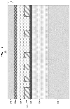
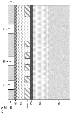
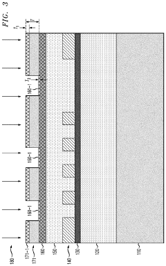
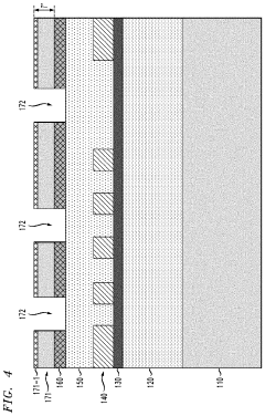
Mask for extreme ultraviolet lithography process and method of fabricating the same
PatentActiveUS10061190B2
Innovation
- A mask for EUV lithography is designed with a substrate, alternately stacked reflection layers, a capping layer, a phase shift layer, and an absorber layer, where the sidewalls of the phase shift and absorber layers are oblique to the top surface of the capping layer, with controlled angles to optimize NILS and CD bias values, and the layers are fabricated using materials with specific refractive indices and absorption coefficients to maintain a total thickness of 40 nm, allowing for precise control of reflectivity and image contrast.


EUV Lithography Industry Standards and Regulations
The EUV lithography industry operates under a complex framework of international standards and regulations that directly impact pattern collapse mitigation strategies. The International Technology Roadmap for Semiconductors (ITRS) and its successor, the International Roadmap for Devices and Systems (IRDS), establish critical dimensional tolerances and defect density requirements that manufacturers must achieve to prevent pattern collapse in sub-7nm processes.
ISO 14996 and SEMI standards define the specifications for EUV resist materials, including mechanical properties such as elastic modulus and adhesion strength that are crucial for pattern stability. These standards mandate minimum resist film integrity requirements and establish testing protocols for evaluating collapse resistance under various processing conditions. Compliance with these specifications ensures that resist formulations can withstand the capillary forces encountered during development and cleaning processes.
The SEMI E127 standard specifically addresses contamination control in EUV systems, which is essential for pattern collapse prevention. Molecular contamination can alter resist chemistry and mechanical properties, leading to weakened pattern structures. This standard establishes acceptable contamination levels for various chemical species and requires implementation of real-time monitoring systems to maintain clean processing environments.
Regulatory frameworks from organizations such as the FDA and EPA govern the use of chemical additives in resist formulations, including surfactants and mechanical reinforcement agents used to prevent pattern collapse. These regulations ensure that new chemical solutions for collapse mitigation undergo proper safety and environmental impact assessments before implementation in manufacturing environments.
International export control regulations, particularly those governing EUV technology transfer, influence the development and deployment of pattern collapse mitigation solutions. The Wassenaar Arrangement and national export control laws restrict the sharing of advanced lithography technologies, affecting collaborative research efforts and standardization processes across different regions.
Quality management standards such as ISO 9001 and automotive-specific IATF 16949 require semiconductor manufacturers to implement systematic approaches to defect prevention, including pattern collapse mitigation. These standards mandate documentation of process controls, statistical process monitoring, and continuous improvement methodologies that directly support the development and implementation of collapse prevention strategies in production environments.
Environmental Impact of EUV Manufacturing Processes
The environmental implications of EUV manufacturing processes present significant challenges that intersect with pattern collapse mitigation strategies. EUV lithography systems require substantial energy consumption, primarily due to the high-power laser systems needed to generate EUV photons through laser-produced plasma sources. These systems typically consume 200-300 kW of electrical power, resulting in considerable carbon footprint concerns for semiconductor manufacturing facilities.
Chemical waste generation represents another critical environmental consideration. The photoresist materials used in EUV lithography, particularly chemically amplified resists designed to address pattern collapse issues, often contain environmentally sensitive compounds. The development and etching processes generate organic solvent waste streams that require specialized treatment and disposal protocols. Advanced resist formulations incorporating metal-containing photoacid generators or molecular glass resists may introduce additional heavy metal contamination risks.
Water consumption in EUV manufacturing processes is substantial, particularly for cooling systems and wet chemical processing steps. The precision cleaning requirements for EUV masks and wafers demand ultra-pure water systems, leading to significant water treatment and recycling challenges. Pattern collapse mitigation techniques that rely on supercritical drying or freeze-drying processes can reduce water-related environmental impacts compared to conventional wet processing methods.
Atmospheric emissions from EUV facilities include volatile organic compounds from photoresist processing and potential ozone depletion substances from cleaning processes. The tin debris generated in EUV light sources creates additional waste management requirements, as tin contamination must be carefully controlled and recycled where possible.
Sustainable manufacturing approaches are emerging to address these environmental challenges. Energy recovery systems can capture waste heat from EUV sources for facility heating applications. Advanced resist recycling technologies are being developed to minimize chemical waste generation. Green chemistry initiatives focus on developing environmentally benign resist formulations that maintain pattern fidelity while reducing ecological impact. Life cycle assessment methodologies are increasingly applied to evaluate the total environmental cost of different pattern collapse mitigation strategies, enabling more informed decision-making in process development.
Unlock deeper insights with Patsnap Eureka Quick Research — get a full tech report to explore trends and direct your research. Try now!
Generate Your Research Report Instantly with AI Agent
Supercharge your innovation with Patsnap Eureka AI Agent Platform!