
EUV Lithography vs Ion Beam Lithography: Yield Comparisons
APR 2, 20269 MIN READ
Generate Your Research Report Instantly with AI Agent
Patsnap Eureka helps you evaluate technical feasibility & market potential.
EUV vs Ion Beam Lithography Background and Yield Targets
Extreme Ultraviolet (EUV) lithography and Ion Beam Lithography (IBL) represent two distinct approaches to next-generation semiconductor manufacturing, each emerging from different technological foundations to address the industry's relentless pursuit of smaller feature sizes. EUV lithography evolved from decades of research into short-wavelength light sources, utilizing 13.5 nm wavelength radiation to achieve sub-10nm patterning capabilities. This technology builds upon traditional optical lithography principles while overcoming the physical limitations imposed by longer wavelengths used in previous generations of photolithography systems.
Ion Beam Lithography, conversely, developed from electron beam lithography concepts, employing focused ion beams for direct-write patterning and mask repair applications. IBL technology leverages the precise control of charged particle beams to achieve exceptional resolution and accuracy, particularly in specialized manufacturing scenarios where flexibility and precision outweigh throughput considerations.
The semiconductor industry's transition toward advanced nodes below 7nm has intensified the demand for lithography solutions capable of maintaining high manufacturing yields while achieving unprecedented pattern fidelity. Current industry targets for EUV lithography focus on achieving production yields exceeding 90% for high-volume manufacturing of logic devices at 5nm and 3nm nodes. These yield requirements encompass defect density targets below 0.1 defects per square centimeter and critical dimension uniformity within ±2nm across entire wafer surfaces.
For Ion Beam Lithography applications, yield targets vary significantly based on specific use cases. In mask repair operations, IBL systems target defect correction success rates above 95% while maintaining original mask specifications. For direct-write applications, yield considerations center on pattern placement accuracy within ±5nm and feature size control better than ±1nm, particularly critical for photomask manufacturing and specialized device prototyping.
The evolution of both technologies reflects the industry's broader shift toward more sophisticated process control and metrology systems. EUV lithography development has progressed through multiple generations of source power improvements, from initial 80W systems to current 250W+ sources, directly impacting achievable throughput and economic viability. Meanwhile, IBL technology has advanced through enhanced beam control systems and improved ion source stability, enabling more reliable and repeatable patterning results across diverse substrate materials and device architectures.
Ion Beam Lithography, conversely, developed from electron beam lithography concepts, employing focused ion beams for direct-write patterning and mask repair applications. IBL technology leverages the precise control of charged particle beams to achieve exceptional resolution and accuracy, particularly in specialized manufacturing scenarios where flexibility and precision outweigh throughput considerations.
The semiconductor industry's transition toward advanced nodes below 7nm has intensified the demand for lithography solutions capable of maintaining high manufacturing yields while achieving unprecedented pattern fidelity. Current industry targets for EUV lithography focus on achieving production yields exceeding 90% for high-volume manufacturing of logic devices at 5nm and 3nm nodes. These yield requirements encompass defect density targets below 0.1 defects per square centimeter and critical dimension uniformity within ±2nm across entire wafer surfaces.
For Ion Beam Lithography applications, yield targets vary significantly based on specific use cases. In mask repair operations, IBL systems target defect correction success rates above 95% while maintaining original mask specifications. For direct-write applications, yield considerations center on pattern placement accuracy within ±5nm and feature size control better than ±1nm, particularly critical for photomask manufacturing and specialized device prototyping.
The evolution of both technologies reflects the industry's broader shift toward more sophisticated process control and metrology systems. EUV lithography development has progressed through multiple generations of source power improvements, from initial 80W systems to current 250W+ sources, directly impacting achievable throughput and economic viability. Meanwhile, IBL technology has advanced through enhanced beam control systems and improved ion source stability, enabling more reliable and repeatable patterning results across diverse substrate materials and device architectures.
Market Demand for Advanced Lithography Solutions
The global semiconductor industry faces unprecedented demand for advanced lithography solutions as device manufacturers push toward smaller node technologies. The transition to sub-7nm processes has created critical requirements for lithography systems capable of achieving higher resolution, improved pattern fidelity, and enhanced manufacturing yields. This demand surge stems from multiple technology sectors including artificial intelligence processors, high-performance computing chips, and advanced mobile processors that require increasingly sophisticated manufacturing capabilities.
Market dynamics reveal a concentrated demand pattern primarily driven by leading foundries and memory manufacturers. Taiwan Semiconductor Manufacturing Company, Samsung, and Intel represent the primary demand generators, collectively accounting for the majority of advanced lithography equipment procurement. These companies require lithography solutions that can deliver consistent sub-10nm patterning with acceptable defect rates and throughput levels to maintain competitive manufacturing economics.
The automotive semiconductor segment has emerged as an additional demand driver, particularly for power management and sensor applications requiring precise geometric control. Electric vehicle adoption and autonomous driving technologies necessitate specialized semiconductor components with stringent reliability requirements, creating sustained demand for advanced lithography capabilities beyond traditional consumer electronics applications.
Cost considerations significantly influence market demand patterns. While EUV lithography systems command premium pricing due to their technical complexity and limited supplier base, the total cost of ownership calculations often favor EUV adoption for high-volume production scenarios. Ion beam lithography, despite lower equipment costs, faces throughput limitations that restrict its application to specialized low-volume or research applications.
Geographic demand distribution shows concentration in Asia-Pacific regions, particularly Taiwan, South Korea, and China, where major semiconductor manufacturing facilities operate. Government initiatives supporting domestic semiconductor capabilities have intensified regional demand, with substantial investments planned for advanced manufacturing infrastructure development.
The market exhibits strong correlation between lithography demand and overall semiconductor capital expenditure cycles. Economic uncertainties and geopolitical factors create demand volatility, yet the fundamental technology transition toward advanced nodes ensures sustained long-term growth prospects for sophisticated lithography solutions capable of meeting stringent yield and performance requirements.
Market dynamics reveal a concentrated demand pattern primarily driven by leading foundries and memory manufacturers. Taiwan Semiconductor Manufacturing Company, Samsung, and Intel represent the primary demand generators, collectively accounting for the majority of advanced lithography equipment procurement. These companies require lithography solutions that can deliver consistent sub-10nm patterning with acceptable defect rates and throughput levels to maintain competitive manufacturing economics.
The automotive semiconductor segment has emerged as an additional demand driver, particularly for power management and sensor applications requiring precise geometric control. Electric vehicle adoption and autonomous driving technologies necessitate specialized semiconductor components with stringent reliability requirements, creating sustained demand for advanced lithography capabilities beyond traditional consumer electronics applications.
Cost considerations significantly influence market demand patterns. While EUV lithography systems command premium pricing due to their technical complexity and limited supplier base, the total cost of ownership calculations often favor EUV adoption for high-volume production scenarios. Ion beam lithography, despite lower equipment costs, faces throughput limitations that restrict its application to specialized low-volume or research applications.
Geographic demand distribution shows concentration in Asia-Pacific regions, particularly Taiwan, South Korea, and China, where major semiconductor manufacturing facilities operate. Government initiatives supporting domestic semiconductor capabilities have intensified regional demand, with substantial investments planned for advanced manufacturing infrastructure development.
The market exhibits strong correlation between lithography demand and overall semiconductor capital expenditure cycles. Economic uncertainties and geopolitical factors create demand volatility, yet the fundamental technology transition toward advanced nodes ensures sustained long-term growth prospects for sophisticated lithography solutions capable of meeting stringent yield and performance requirements.
Current Yield Challenges in EUV and Ion Beam Technologies
EUV lithography faces significant yield challenges primarily stemming from photon shot noise, which becomes increasingly problematic at advanced nodes below 7nm. The stochastic nature of photon distribution creates random variations in resist exposure, leading to line edge roughness, critical dimension uniformity issues, and pattern collapse. These stochastic effects directly impact yield by causing devices to fall outside acceptable performance parameters, with defect densities often exceeding industry targets for high-volume manufacturing.
Mask defects represent another critical yield limitation for EUV systems. The reflective multilayer masks are extremely sensitive to particle contamination and defects, which can be amplified during the lithographic process. Pellicle technology, commonly used in DUV systems for mask protection, remains immature for EUV applications due to thermal management challenges, leaving masks vulnerable to contamination during exposure.
Source power stability and availability constitute ongoing yield challenges for EUV lithography. Current generation EUV sources operate at approximately 250W, requiring continuous optimization to maintain consistent dose delivery. Power fluctuations and source downtime directly translate to throughput losses and yield variations, as exposure dose uniformity across wafers becomes compromised.
Ion beam lithography encounters distinct yield challenges related to proximity effects and charging phenomena. The interaction between incident ions and substrate materials creates secondary electron generation, leading to unwanted exposure in adjacent areas. This proximity effect becomes more severe with increasing pattern density, causing critical dimension variations and pattern distortion that negatively impact yield, particularly in dense memory and logic structures.
Charging effects in ion beam systems pose significant yield risks, especially when processing insulating materials or partially processed wafers with varying conductivity. Charge accumulation can deflect the ion beam, causing placement errors and dose variations that result in pattern defects. These charging effects are particularly problematic in multi-layer processing scenarios common in advanced semiconductor manufacturing.
Throughput limitations in ion beam lithography create indirect yield challenges through extended processing times. The serial nature of ion beam writing, while offering excellent resolution control, results in significantly longer exposure times compared to parallel exposure systems. Extended processing increases the probability of contamination, vibration-induced errors, and system drift, all contributing to reduced yield performance in high-volume manufacturing environments.
Mask defects represent another critical yield limitation for EUV systems. The reflective multilayer masks are extremely sensitive to particle contamination and defects, which can be amplified during the lithographic process. Pellicle technology, commonly used in DUV systems for mask protection, remains immature for EUV applications due to thermal management challenges, leaving masks vulnerable to contamination during exposure.
Source power stability and availability constitute ongoing yield challenges for EUV lithography. Current generation EUV sources operate at approximately 250W, requiring continuous optimization to maintain consistent dose delivery. Power fluctuations and source downtime directly translate to throughput losses and yield variations, as exposure dose uniformity across wafers becomes compromised.
Ion beam lithography encounters distinct yield challenges related to proximity effects and charging phenomena. The interaction between incident ions and substrate materials creates secondary electron generation, leading to unwanted exposure in adjacent areas. This proximity effect becomes more severe with increasing pattern density, causing critical dimension variations and pattern distortion that negatively impact yield, particularly in dense memory and logic structures.
Charging effects in ion beam systems pose significant yield risks, especially when processing insulating materials or partially processed wafers with varying conductivity. Charge accumulation can deflect the ion beam, causing placement errors and dose variations that result in pattern defects. These charging effects are particularly problematic in multi-layer processing scenarios common in advanced semiconductor manufacturing.
Throughput limitations in ion beam lithography create indirect yield challenges through extended processing times. The serial nature of ion beam writing, while offering excellent resolution control, results in significantly longer exposure times compared to parallel exposure systems. Extended processing increases the probability of contamination, vibration-induced errors, and system drift, all contributing to reduced yield performance in high-volume manufacturing environments.
Current Yield Enhancement Solutions and Methodologies
01 EUV mask defect inspection and repair techniques
Extreme ultraviolet lithography requires advanced mask defect detection and repair methods to improve yield. Techniques include actinic inspection systems that use EUV wavelengths to identify defects, and repair methods using focused ion beams or other localized material removal processes. These approaches help identify and correct mask defects that could impact pattern transfer quality and overall manufacturing yield.- EUV mask defect inspection and repair techniques: Extreme ultraviolet lithography requires advanced mask defect inspection and repair methods to improve yield. Techniques include using specialized inspection tools to detect defects at nanometer scale, implementing actinic inspection systems that use EUV wavelengths for accurate defect detection, and developing repair strategies for both absorber and multilayer defects. These methods help identify and correct mask defects before production, significantly reducing pattern transfer errors and improving overall lithography yield.
- Ion beam processing for pattern correction and edge placement: Ion beam lithography and processing techniques are employed to enhance pattern fidelity and correct edge placement errors. Methods include using focused ion beams for direct pattern writing, implementing ion beam etching for precise feature definition, and applying ion beam-induced deposition for pattern repair. These techniques enable sub-nanometer precision in pattern placement and can correct defects that occur during initial lithography steps, thereby improving final device yield.
- Resist material optimization for EUV and ion beam lithography: Development of specialized resist materials tailored for extreme ultraviolet and ion beam exposure improves pattern resolution and reduces defects. Advanced resist formulations include chemically amplified resists with optimized sensitivity, metal-containing resists for enhanced absorption, and materials with reduced line edge roughness. Proper resist selection and processing conditions are critical for achieving high-quality patterns and maximizing manufacturing yield in advanced lithography processes.
- Overlay and alignment control systems: Precise overlay and alignment control mechanisms are essential for maintaining yield in multi-layer patterning processes. Technologies include advanced metrology systems for measuring overlay errors, real-time feedback control for alignment correction, and computational methods for predicting and compensating overlay drift. These systems ensure accurate layer-to-layer registration, which is critical for device functionality and directly impacts manufacturing yield in both lithography techniques.
- Contamination control and particle reduction methods: Controlling contamination and reducing particle generation during lithography processes is crucial for yield improvement. Strategies include implementing clean room protocols, using particle detection systems, developing self-cleaning optical components, and optimizing vacuum systems to minimize outgassing. Contamination on masks or wafers can cause critical defects, so maintaining ultra-clean processing environments and implementing effective particle mitigation strategies are essential for achieving high yield in advanced lithography.
02 Ion beam lithography patterning optimization
Ion beam lithography systems utilize focused ion beams for direct-write patterning or mask repair applications. Optimization techniques include beam current control, dose modulation, and proximity effect correction to achieve high-resolution patterns with minimal defects. Advanced beam shaping and scanning strategies improve throughput while maintaining pattern fidelity, directly contributing to enhanced lithography yield.Expand Specific Solutions03 EUV source power and stability enhancement
Increasing the power output and stability of EUV light sources is critical for improving lithography throughput and yield. Methods include optimized laser-produced plasma or discharge-produced plasma sources, debris mitigation systems, and collector optics with enhanced reflectivity. Stable and high-power EUV sources reduce exposure time variations and improve pattern uniformity across wafers.Expand Specific Solutions04 Resist materials and processing for advanced lithography
Development of specialized photoresist and resist processing techniques tailored for EUV and ion beam lithography improves pattern resolution and reduces defects. This includes chemically amplified resists with optimized sensitivity, line edge roughness reduction methods, and post-exposure processing techniques. Advanced resist materials enable better pattern transfer and contribute to higher manufacturing yields.Expand Specific Solutions05 Metrology and process control for yield improvement
Advanced metrology systems and process control methods are essential for monitoring and optimizing lithography performance. Techniques include in-situ monitoring of critical dimensions, overlay measurements, and real-time feedback control systems. Integration of machine learning algorithms for defect classification and process optimization enables predictive maintenance and adaptive process control, leading to sustained yield improvements.Expand Specific Solutions
Key Players in EUV and Ion Beam Lithography Markets
The EUV versus Ion Beam lithography competition represents a mature semiconductor manufacturing landscape where EUV has achieved commercial dominance while ion beam remains specialized. The market, valued at billions globally, is driven by advanced node requirements below 7nm. EUV technology has reached production maturity, with ASML Holding NV monopolizing EUV systems, while foundries like TSMC, Samsung Electronics, and GlobalFoundries deploy these systems for high-volume manufacturing. Ion beam lithography, though offering superior resolution, remains limited to specialized applications due to throughput constraints. Key players include equipment manufacturers like Tokyo Electron, Applied Materials, and Nikon for conventional systems, while materials suppliers such as Shin-Etsu Chemical and AGC provide critical components. Research institutions like MIT and Osaka University continue advancing both technologies, but commercial momentum heavily favors EUV for mainstream production.
Taiwan Semiconductor Manufacturing Co., Ltd.
Technical Solution: TSMC has extensively implemented EUV lithography for advanced node production, achieving industry-leading yields at 5nm and 3nm processes. The company reports EUV yield rates exceeding 90% for mature 7nm processes and continuously improving yields for 3nm production. TSMC's approach focuses on optimizing EUV exposure conditions, implementing advanced computational lithography, and developing proprietary defect reduction techniques. While the company has limited public research on ion beam lithography for production, they maintain evaluation programs for emerging lithography technologies. Their EUV implementation strategy emphasizes high-volume manufacturing readiness and cost-effective production scaling.
Strengths: Industry-leading EUV production yields, extensive manufacturing experience, strong process optimization capabilities. Weaknesses: Heavy dependence on EUV supplier ecosystem, limited ion beam lithography production experience, high capital investment requirements.
ASML Netherlands BV
Technical Solution: ASML dominates EUV lithography equipment supply with their NXE series systems, achieving throughput improvements from 125 wafers per hour to over 160 wafers per hour in latest generations. The company reports significant yield improvements through enhanced source power, improved optics stability, and advanced pellicle technology. ASML's EUV systems demonstrate defectivity levels below 0.1 defects per cm² for critical layers. While primarily focused on EUV, ASML has research partnerships exploring alternative lithography approaches including ion beam applications for specific patterning challenges. Their roadmap includes next-generation EUV systems targeting even higher yields and throughput for sub-3nm nodes.
Strengths: Market-leading EUV technology, continuous yield improvements, comprehensive ecosystem support. Weaknesses: Limited ion beam lithography portfolio, complex system maintenance requirements, high equipment costs affecting customer adoption.
Core Patents in Lithography Yield Improvement Technologies
EUVL precision component with specific thermal expansion behavior
PatentPendingUS20240077798A1
Innovation
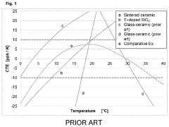
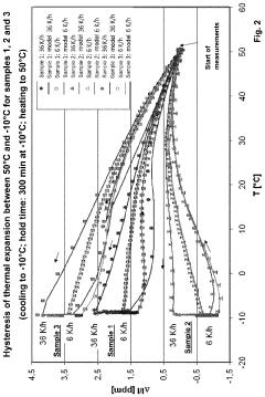
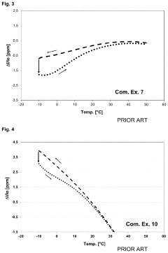
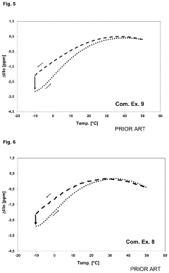
- A precision EUVL component with an average CTE of at most 0±0.1×10⁻⁶/K and thermal hysteresis of <0.1 ppm in the temperature range from 19 to 25°C, utilizing an LAS glass-ceramic composition with optimized SiO2, Li2O, and nucleating agents like TiO2, ZrO2, and WO3, which minimizes thermal hysteresis and ensures zero expansion.
Method of simulating resist pattern, resist material and method of optimizing formulation thereof, apparatus and recording medium
PatentActiveUS20200057371A1
Innovation
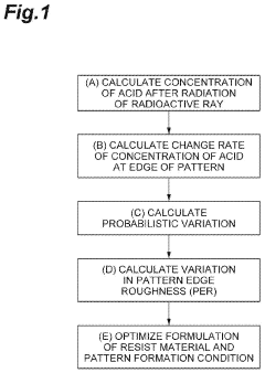
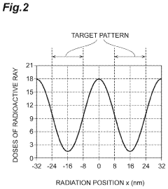
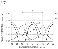
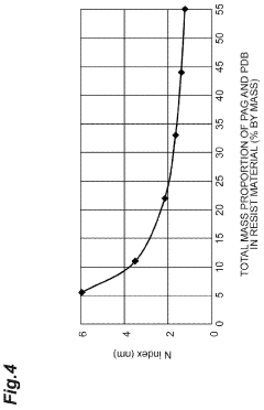
- A simulation method and resist material formulation optimization that accounts for probabilistic variations in photon noise and active species distribution, using a chemical amplification-type resist material with a photo-acid-generating agent and photodecomposable quencher, to minimize pattern edge roughness and sensitivity variations.
Semiconductor Manufacturing Standards and Regulations
The semiconductor manufacturing industry operates under a comprehensive framework of standards and regulations that directly impact the implementation and yield optimization of advanced lithography technologies, including EUV and ion beam lithography. These regulatory frameworks establish critical parameters for process control, contamination limits, and quality assurance protocols that significantly influence the comparative performance of different lithography approaches.
International standards organizations, particularly SEMI (Semiconductor Equipment and Materials International) and ISO (International Organization for Standardization), have developed specific guidelines for advanced lithography processes. SEMI E10 standards define environmental requirements for cleanroom operations, while SEMI E49 establishes guidelines for process equipment automation that are crucial for maintaining consistent yields in both EUV and ion beam lithography systems. These standards mandate specific particle contamination limits, with Class 1 cleanroom requirements becoming increasingly stringent as feature sizes decrease below 7nm nodes.
Regulatory compliance frameworks vary significantly between regions, with the United States, European Union, and Asia-Pacific markets each maintaining distinct requirements for semiconductor manufacturing processes. The FDA's semiconductor device regulations in medical applications, EU's RoHS directives for material restrictions, and Japan's industrial safety standards all impose specific constraints on lithography equipment design and operation protocols. These regional variations create complexity in yield comparison studies, as identical lithography systems may perform differently under varying regulatory constraints.
Quality management standards, particularly ISO 9001 and automotive-specific IATF 16949, establish mandatory process control requirements that affect yield measurement methodologies. These standards require statistical process control implementation, defect tracking protocols, and continuous improvement documentation that directly influence how EUV and ion beam lithography yields are measured, reported, and compared across different manufacturing facilities.
Environmental and safety regulations increasingly impact lithography technology selection and implementation. EUV systems face specific regulatory challenges related to hydrogen gas handling, extreme ultraviolet radiation safety protocols, and tin debris management systems. Ion beam lithography encounters different regulatory requirements concerning ion source materials, vacuum system safety, and electromagnetic field exposure limits. These regulatory differences create additional variables in yield comparison analyses, as compliance costs and operational constraints vary significantly between the two technologies.
Emerging regulations addressing supply chain security, particularly in critical semiconductor applications, are beginning to influence lithography technology adoption decisions. Export control regulations and technology transfer restrictions may limit access to specific lithography solutions, potentially affecting yield optimization strategies and creating regional disparities in manufacturing capabilities and performance benchmarks.
International standards organizations, particularly SEMI (Semiconductor Equipment and Materials International) and ISO (International Organization for Standardization), have developed specific guidelines for advanced lithography processes. SEMI E10 standards define environmental requirements for cleanroom operations, while SEMI E49 establishes guidelines for process equipment automation that are crucial for maintaining consistent yields in both EUV and ion beam lithography systems. These standards mandate specific particle contamination limits, with Class 1 cleanroom requirements becoming increasingly stringent as feature sizes decrease below 7nm nodes.
Regulatory compliance frameworks vary significantly between regions, with the United States, European Union, and Asia-Pacific markets each maintaining distinct requirements for semiconductor manufacturing processes. The FDA's semiconductor device regulations in medical applications, EU's RoHS directives for material restrictions, and Japan's industrial safety standards all impose specific constraints on lithography equipment design and operation protocols. These regional variations create complexity in yield comparison studies, as identical lithography systems may perform differently under varying regulatory constraints.
Quality management standards, particularly ISO 9001 and automotive-specific IATF 16949, establish mandatory process control requirements that affect yield measurement methodologies. These standards require statistical process control implementation, defect tracking protocols, and continuous improvement documentation that directly influence how EUV and ion beam lithography yields are measured, reported, and compared across different manufacturing facilities.
Environmental and safety regulations increasingly impact lithography technology selection and implementation. EUV systems face specific regulatory challenges related to hydrogen gas handling, extreme ultraviolet radiation safety protocols, and tin debris management systems. Ion beam lithography encounters different regulatory requirements concerning ion source materials, vacuum system safety, and electromagnetic field exposure limits. These regulatory differences create additional variables in yield comparison analyses, as compliance costs and operational constraints vary significantly between the two technologies.
Emerging regulations addressing supply chain security, particularly in critical semiconductor applications, are beginning to influence lithography technology adoption decisions. Export control regulations and technology transfer restrictions may limit access to specific lithography solutions, potentially affecting yield optimization strategies and creating regional disparities in manufacturing capabilities and performance benchmarks.
Cost-Benefit Analysis of EUV vs Ion Beam Approaches
The economic evaluation of EUV lithography versus ion beam lithography reveals significant disparities in capital expenditure, operational costs, and return on investment profiles. EUV systems require substantial upfront investments, with leading-edge scanners costing approximately $200-300 million per unit, while ion beam lithography systems typically range from $50-100 million depending on configuration and throughput capabilities.
Operational expenditure analysis demonstrates contrasting cost structures between the two approaches. EUV lithography incurs high consumable costs, particularly for photoresist materials and pellicle replacements, alongside substantial power consumption averaging 1-2 MW per scanner. The technology also demands expensive infrastructure modifications including specialized cleanroom environments and advanced metrology systems. Conversely, ion beam systems exhibit lower power requirements but face challenges with slower throughput rates, resulting in higher per-wafer processing costs for high-volume manufacturing scenarios.
Throughput economics significantly impact the cost-benefit equation. EUV systems achieve wafer processing rates of 140-170 wafers per hour for advanced nodes, enabling economies of scale that justify premium equipment costs in high-volume production environments. Ion beam lithography, while offering superior precision and defect control, typically processes 20-40 wafers per hour, making it economically viable primarily for specialized applications, prototyping, or low-volume production runs where precision requirements outweigh throughput considerations.
The total cost of ownership analysis over a five-year operational period reveals that EUV becomes cost-effective when annual wafer volumes exceed approximately 50,000 units for 7nm and below process nodes. Below this threshold, ion beam approaches demonstrate superior economic performance, particularly when factoring in reduced mask costs and simplified process integration requirements. Additionally, ion beam systems offer greater flexibility for research and development applications, providing better return on investment for organizations prioritizing technological exploration over volume manufacturing.
Risk-adjusted financial modeling indicates that EUV investments carry higher technological obsolescence risks but offer greater scalability potential, while ion beam systems provide more predictable cost structures with lower capital exposure, making them attractive for specialized market segments and emerging technology development initiatives.
Operational expenditure analysis demonstrates contrasting cost structures between the two approaches. EUV lithography incurs high consumable costs, particularly for photoresist materials and pellicle replacements, alongside substantial power consumption averaging 1-2 MW per scanner. The technology also demands expensive infrastructure modifications including specialized cleanroom environments and advanced metrology systems. Conversely, ion beam systems exhibit lower power requirements but face challenges with slower throughput rates, resulting in higher per-wafer processing costs for high-volume manufacturing scenarios.
Throughput economics significantly impact the cost-benefit equation. EUV systems achieve wafer processing rates of 140-170 wafers per hour for advanced nodes, enabling economies of scale that justify premium equipment costs in high-volume production environments. Ion beam lithography, while offering superior precision and defect control, typically processes 20-40 wafers per hour, making it economically viable primarily for specialized applications, prototyping, or low-volume production runs where precision requirements outweigh throughput considerations.
The total cost of ownership analysis over a five-year operational period reveals that EUV becomes cost-effective when annual wafer volumes exceed approximately 50,000 units for 7nm and below process nodes. Below this threshold, ion beam approaches demonstrate superior economic performance, particularly when factoring in reduced mask costs and simplified process integration requirements. Additionally, ion beam systems offer greater flexibility for research and development applications, providing better return on investment for organizations prioritizing technological exploration over volume manufacturing.
Risk-adjusted financial modeling indicates that EUV investments carry higher technological obsolescence risks but offer greater scalability potential, while ion beam systems provide more predictable cost structures with lower capital exposure, making them attractive for specialized market segments and emerging technology development initiatives.
Unlock deeper insights with Patsnap Eureka Quick Research — get a full tech report to explore trends and direct your research. Try now!
Generate Your Research Report Instantly with AI Agent
Supercharge your innovation with Patsnap Eureka AI Agent Platform!