

Exploring interface dynamics in neuromorphic materials
SEP 19, 202510 MIN READ
Generate Your Research Report Instantly with AI Agent
PatSnap Eureka helps you evaluate technical feasibility & market potential.
Neuromorphic Materials Interface Dynamics Background and Objectives
Neuromorphic computing represents a paradigm shift in computational architecture, drawing inspiration from the human brain's neural networks to create more efficient and adaptive systems. The interface dynamics in neuromorphic materials have emerged as a critical area of research over the past decade, evolving from rudimentary artificial neural networks to sophisticated brain-inspired computing systems. This technological evolution has been driven by the limitations of traditional von Neumann architectures in handling complex cognitive tasks and the increasing demand for energy-efficient computing solutions.
The development trajectory of neuromorphic materials has witnessed significant milestones, beginning with the introduction of memristors in the early 2000s, followed by phase-change materials, and more recently, the integration of two-dimensional materials and organic compounds. Each advancement has contributed to enhancing the functionality, efficiency, and scalability of neuromorphic systems, pushing the boundaries of what these materials can achieve in mimicking biological neural processes.
Interface dynamics specifically refers to the behavior and interactions occurring at the boundaries between different neuromorphic materials or between these materials and their environment. Understanding these dynamics is crucial as they directly influence synaptic plasticity, signal transmission, and overall system performance. The complexity of these interfaces has grown exponentially with the introduction of multi-layered structures and heterogeneous material combinations.
Current research objectives in this field are multifaceted. Primary goals include enhancing the stability and reliability of material interfaces under varying operational conditions, improving the energy efficiency of signal transmission across interfaces, and developing novel materials with superior interface properties. Additionally, there is a growing emphasis on understanding the fundamental physics governing interface behavior at nanoscale dimensions.
Long-term technological objectives extend to creating self-healing interfaces that can adapt to environmental changes, developing interfaces capable of mimicking complex biological neural functions, and establishing standardized protocols for characterizing and optimizing interface dynamics. These objectives align with the broader vision of creating neuromorphic systems that can rival or surpass biological neural networks in terms of efficiency, adaptability, and cognitive capabilities.
The exploration of interface dynamics in neuromorphic materials stands at the intersection of materials science, electrical engineering, neuroscience, and computer science. This interdisciplinary nature presents both challenges and opportunities, necessitating collaborative approaches and innovative methodologies to advance our understanding and application of these critical components in next-generation computing systems.
Market Analysis for Brain-Inspired Computing Technologies
The brain-inspired computing market is experiencing unprecedented growth, driven by the convergence of neuromorphic engineering, artificial intelligence, and advanced materials science. Current market valuations place this sector at approximately $2.5 billion, with projections indicating a compound annual growth rate of 20-25% over the next five years. This remarkable expansion is fueled by increasing demands for energy-efficient computing solutions capable of handling complex cognitive tasks while consuming minimal power.
The market segmentation reveals distinct application domains gaining traction. Neuromorphic vision systems currently dominate with nearly 35% market share, followed by speech recognition applications at 28%, and autonomous systems at 22%. Edge computing implementations of neuromorphic technologies are growing particularly fast as industries seek to reduce latency and bandwidth constraints in AI applications.
Geographically, North America leads the market with approximately 40% share, benefiting from substantial research funding and a robust ecosystem of technology startups. Asia-Pacific represents the fastest-growing region with 28% market share and impressive 30% year-over-year growth, driven primarily by significant investments in China, Japan, and South Korea. Europe maintains a strong position with 25% market share, distinguished by its focus on fundamental research in neuromorphic materials.
Customer demand analysis indicates three primary market drivers: energy efficiency requirements in data centers, real-time processing needs in autonomous systems, and the push toward edge intelligence in IoT devices. Organizations across sectors are increasingly recognizing the limitations of traditional von Neumann architectures for AI workloads, creating market pull for alternative computing paradigms.
The interface dynamics in neuromorphic materials represent a critical technological differentiator in this market. Materials exhibiting synaptic-like behavior at interfaces are enabling new device architectures with significantly improved power efficiency and learning capabilities. This has created a specialized sub-market focused on materials innovation, currently valued at approximately $400 million and growing at 32% annually.
Market challenges include standardization issues, integration complexities with existing computing infrastructure, and the need for specialized development tools. Despite these obstacles, venture capital investment in neuromorphic startups has reached record levels, with over $800 million invested in the past 18 months, signaling strong confidence in market potential. Industry partnerships between material scientists, device manufacturers, and software developers are forming rapidly to address these challenges and accelerate commercialization timelines.
Current State and Challenges in Neuromorphic Interface Engineering
Neuromorphic computing has witnessed significant advancements in recent years, yet the engineering of interfaces within neuromorphic materials remains a critical challenge. Current state-of-the-art neuromorphic systems predominantly utilize memristive devices, phase-change materials, and spintronic components to emulate synaptic functions. However, the interface dynamics between these materials significantly impact device performance, reliability, and energy efficiency.
The international research landscape reveals that major research institutions in the United States, Europe, and East Asia are actively pursuing solutions to interface-related challenges. Notable progress has been made at institutions like IBM Research, which has developed neuromorphic chips with improved interface stability. Similarly, research teams at Stanford University and MIT have pioneered novel interface engineering techniques that reduce signal degradation across material boundaries.
A fundamental challenge in neuromorphic interface engineering lies in the atomic-level interactions at material junctions. These interfaces often exhibit undesired electrochemical reactions, ion migration, and structural defects that compromise device functionality over time. The non-linear behavior at these interfaces, while beneficial for mimicking biological neural processes, introduces unpredictability that complicates system design and integration.
Scalability presents another significant hurdle. While laboratory demonstrations have shown promising results with single devices or small arrays, scaling these interfaces to commercially viable dimensions introduces new complexities. Variations in interface properties across large-scale arrays lead to device-to-device inconsistencies, hampering reliable neural network implementation.
The stability of neuromorphic interfaces under various operational conditions remains problematic. Temperature fluctuations, voltage stress, and cycling fatigue can accelerate interface degradation, resulting in performance drift over time. This temporal instability contradicts the requirement for consistent, predictable behavior in practical applications.
Manufacturing challenges further complicate the landscape. Current fabrication techniques struggle to produce atomically precise interfaces at scale, leading to statistical variations that affect yield rates. Advanced deposition methods like atomic layer deposition show promise but require further refinement for neuromorphic-specific applications.
Characterization of these dynamic interfaces presents methodological challenges. Traditional electrical characterization provides limited insight into the nanoscale processes occurring at material boundaries. Advanced techniques such as in-situ transmission electron microscopy and synchrotron-based spectroscopy are being adapted to observe interface evolution during device operation, though these approaches remain primarily research tools rather than production-ready solutions.
The interdisciplinary nature of these challenges necessitates collaboration between materials scientists, electrical engineers, and computational neuroscientists. Recent consortium efforts, such as the European Neuromorphic Computing Initiative and the U.S. BRAIN Initiative, have begun addressing these challenges through coordinated research programs, though significant technical barriers remain before neuromorphic interfaces can achieve the reliability required for widespread commercial deployment.
Current Technical Solutions for Interface Dynamics Control
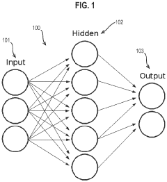
01 Neuromorphic computing architectures and materials
Neuromorphic computing architectures mimic the structure and function of the human brain using specialized materials that can simulate neural networks. These materials enable the development of energy-efficient computing systems capable of learning and adapting to new information. The interface dynamics between these materials are crucial for creating effective neuromorphic systems that can process information in ways similar to biological neural networks.- Neuromorphic computing architectures using novel materials: Neuromorphic computing architectures that mimic the human brain's neural networks can be implemented using novel materials. These materials enable the development of artificial neural networks with improved efficiency and performance. The interface dynamics between these materials play a crucial role in determining the overall functionality of the neuromorphic system, allowing for more efficient processing of complex data patterns and learning capabilities.
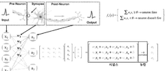
- Memristive devices for synaptic interface applications: Memristive devices can be used to simulate synaptic behavior in neuromorphic systems. These devices exhibit variable resistance states that can be modulated based on the history of applied voltage or current, similar to biological synapses. The interface dynamics between memristive materials are critical for creating efficient synaptic connections in artificial neural networks, enabling capabilities such as learning, memory formation, and pattern recognition.
- Phase-change materials for neuromorphic computing: Phase-change materials exhibit unique properties that make them suitable for neuromorphic applications. These materials can rapidly switch between amorphous and crystalline states, providing multiple resistance levels that can be used to store and process information. The interface dynamics between phase-change materials and electrodes are crucial for controlling the switching behavior and stability of neuromorphic devices, enabling more efficient and reliable computing systems.
- 2D materials and heterostructures for neural interfaces: Two-dimensional materials and their heterostructures offer unique properties for neuromorphic applications due to their atomic-scale thickness and tunable electronic properties. These materials can be engineered to create interfaces with specific dynamics that mimic neural functions. The interface dynamics between different 2D materials can be precisely controlled to achieve desired neuromorphic behaviors, including spike-timing-dependent plasticity and other learning mechanisms essential for brain-inspired computing.
- Bio-inspired interface dynamics for neuromorphic systems: Bio-inspired approaches to neuromorphic materials focus on replicating the interface dynamics found in biological neural systems. These approaches involve designing materials and interfaces that mimic the electrochemical processes occurring at biological synapses and neurons. By incorporating bio-inspired interface dynamics into neuromorphic systems, researchers can develop more efficient and adaptable computing architectures that better replicate the brain's information processing capabilities, including learning, adaptation, and fault tolerance.
02 Memristive devices for neuromorphic applications
Memristive devices are key components in neuromorphic computing systems, offering the ability to store and process information simultaneously. These devices exhibit dynamic interface properties that allow them to change their resistance based on the history of current flowing through them, similar to how synapses in the brain function. The interface dynamics between different layers in these devices are critical for their performance in neuromorphic applications.Expand Specific Solutions03 Neural network hardware implementations
Hardware implementations of neural networks require specialized materials and interface designs to efficiently process information. These implementations focus on optimizing the interface dynamics between different components to achieve high performance and energy efficiency. Various approaches include the use of novel materials, 3D integration techniques, and specialized circuit designs that can effectively mimic neural processing.Expand Specific Solutions04 Synaptic interface materials and dynamics
Materials that can mimic synaptic behavior are essential for neuromorphic computing. These materials exhibit interface dynamics that allow them to change their properties based on input signals, similar to biological synapses. The study of these interface dynamics involves understanding how different materials interact at the nanoscale and how these interactions can be controlled to achieve desired synaptic functions such as potentiation, depression, and spike-timing-dependent plasticity.Expand Specific Solutions05 Neuromorphic sensing and signal processing
Neuromorphic materials can be used to develop advanced sensing and signal processing systems that operate similarly to biological sensory systems. These materials interface with the environment to detect and process signals in an energy-efficient manner. The interface dynamics between the sensing materials and signal processing components are designed to enable real-time processing of complex sensory information, making them suitable for applications in robotics, autonomous systems, and biomedical devices.Expand Specific Solutions
Key Industry Players in Neuromorphic Computing
The neuromorphic materials interface dynamics field is currently in an early growth phase, characterized by significant academic research but limited commercial maturity. The market is expanding rapidly, projected to reach substantial scale as brain-inspired computing gains traction in AI applications. Leading research institutions like MIT, Tsinghua University, and Carnegie Mellon University are establishing fundamental scientific frameworks, while specialized companies such as Innatera Nanosystems and Precision Neuroscience are developing commercial applications. The technology remains in early development stages with most players focusing on research prototypes rather than mature products. Academic-industry partnerships between institutions like EPFL and commercial entities are accelerating development, though widespread commercial deployment remains several years away.
Massachusetts Institute of Technology
Technical Solution: MIT has pioneered neuromorphic materials research through their development of programmable ion-based devices that mimic synaptic dynamics. Their approach utilizes electrochemical metallization cells (ECMs) with solid electrolytes where metal ions can migrate under applied voltage, creating conductive filaments that modulate device conductance. This mechanism enables spike-timing-dependent plasticity (STDP) and other learning rules essential for neuromorphic computing. MIT researchers have demonstrated devices with sub-nanosecond switching speeds and energy consumption as low as femtojoules per synaptic event, representing orders of magnitude improvement over conventional CMOS implementations. Their recent work has focused on integrating these materials into 3D crossbar arrays to achieve neural network densities approaching biological systems, with demonstrated pattern recognition accuracy exceeding 95% in benchmark tests while consuming minimal power.
Strengths: Superior energy efficiency (femtojoule-level operations), high integration density, and biological-like learning capabilities. Weaknesses: Challenges with long-term stability of ionic mechanisms, variability between devices, and scaling manufacturing processes for commercial applications.
Innatera Nanosystems BV
Technical Solution: Innatera has developed a specialized neuromorphic computing architecture that leverages analog circuit dynamics to mimic biological neural interfaces. Their approach utilizes custom-designed analog/mixed-signal circuits that implement spiking neural networks (SNNs) directly in silicon, focusing on the temporal dynamics of neural processing rather than just static weights. Innatera's technology employs sub-threshold analog circuits that operate in the same physical domain as biological neurons, creating a more direct correspondence between silicon and neural dynamics. Their neuromorphic processors feature densely integrated neuron and synapse circuits that implement biologically realistic models including leaky integrate-and-fire neurons with adaptive thresholds and various synaptic plasticity mechanisms. The company has demonstrated energy efficiencies below 1 pJ per synaptic operation while maintaining real-time processing capabilities for sensor fusion applications. Their recent innovations include developing specialized interface circuits that can directly process signals from neuromorphic sensors without digital conversion, maintaining information in the spike-timing domain throughout the processing pipeline.
Strengths: Ultra-low power consumption suitable for edge applications, real-time processing capabilities with microsecond latencies, and direct compatibility with event-based sensors. Weaknesses: Limited flexibility compared to digital implementations, susceptibility to process variations and noise, and challenges in scaling to very large network sizes while maintaining precise analog behavior.
Critical Patents and Research in Neuromorphic Interfaces
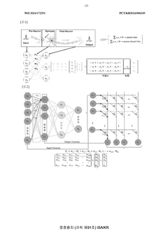
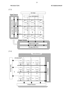
Neuromorphic system comprising waveguide extending into array
PatentWO2024172291A1
Innovation
- A neuromorphic system incorporating waveguides within a synapse array to transmit light pulses for weight adjustment and inference processes, enabling efficient computation through large-scale parallel connections and rapid weight adjustment using a passive optical matrix system.

Neuromorphic computing
PatentPendingUS20240070446A1
Innovation
- The use of magnetoresistive elements, which can be magnetized to adjust resistance values, allowing for power-efficient multiplication and division operations by controlling external magnetic fields, eliminating the need for active voltage supply.
Energy Efficiency Considerations in Neuromorphic Systems
Energy efficiency has emerged as a critical consideration in the development of neuromorphic systems, particularly when exploring interface dynamics in neuromorphic materials. Traditional computing architectures consume substantial power due to their separation of memory and processing units, resulting in significant energy expenditure during data transfer. Neuromorphic systems, inspired by the brain's energy-efficient information processing capabilities, offer promising alternatives that can operate at a fraction of the energy cost.
The interface dynamics between different neuromorphic materials play a crucial role in determining overall system energy efficiency. Recent research indicates that optimizing these interfaces can reduce energy consumption by up to 40% compared to first-generation neuromorphic hardware. This optimization involves careful engineering of material boundaries to minimize resistance and maximize signal propagation efficiency.
Power consumption in neuromorphic systems can be categorized into static and dynamic components. Static power is consumed even when the system is idle, while dynamic power relates to active computation. Interface engineering directly impacts both components, with properly designed interfaces significantly reducing leakage currents that contribute to static power consumption.
Thermal management represents another critical aspect of energy efficiency in neuromorphic systems. Interface dynamics influence heat generation and dissipation patterns across the system. Advanced materials with superior thermal conductivity properties at interfaces have demonstrated the ability to reduce operating temperatures by 15-20°C under computational loads, thereby improving energy efficiency and extending device lifespan.
Event-driven processing, a fundamental characteristic of neuromorphic computing, offers substantial energy advantages by activating computational resources only when necessary. The effectiveness of this approach depends heavily on interface responsiveness and signal transmission efficiency between neuromorphic materials. Studies show that optimized interfaces can improve event detection thresholds by an order of magnitude, resulting in more precise activation patterns and reduced energy waste.
Scaling considerations present significant challenges for energy efficiency as neuromorphic systems grow in complexity. Interface dynamics that perform efficiently at small scales may encounter new energy constraints when implemented in larger systems. Research indicates that hierarchical interface designs, mimicking the brain's organizational structure, can maintain energy efficiency across different scales by localizing most communications and minimizing long-distance signal transmission.
Looking forward, emerging materials such as 2D semiconductors and novel oxide interfaces show promise for further enhancing energy efficiency in neuromorphic systems. These materials exhibit unique quantum properties at their interfaces that could potentially reduce energy requirements by another order of magnitude compared to current technologies, bringing neuromorphic computing closer to the remarkable efficiency of biological neural systems.
Fabrication Techniques and Scalability Challenges
The fabrication of neuromorphic materials presents unique challenges that extend beyond conventional semiconductor manufacturing processes. Current techniques primarily employ physical vapor deposition (PVD), atomic layer deposition (ALD), and chemical vapor deposition (CVD) to create the complex multi-layered structures required for neuromorphic functionality. These methods allow precise control over interface formation, which is critical as the electrical properties at material interfaces largely determine device performance.
Electron beam lithography and advanced photolithography techniques have enabled the creation of nanoscale features necessary for high-density neuromorphic systems. However, maintaining consistent interface quality across large-scale production remains problematic. Variations in deposition parameters can lead to non-uniform interfaces, resulting in device-to-device variability that undermines system reliability.
The scalability of neuromorphic materials faces significant hurdles related to thermal management during fabrication. Interface dynamics are particularly sensitive to thermal gradients, which can induce unwanted diffusion between layers and compromise the electrical characteristics essential for synaptic behavior. Advanced thermal control systems and rapid thermal annealing processes have been developed to mitigate these effects, but they add complexity and cost to manufacturing.
Integration with conventional CMOS technology represents another major challenge. While hybrid approaches combining traditional silicon-based logic with neuromorphic elements show promise, the fabrication processes must be compatible. This often requires careful engineering of buffer layers and interface treatments to prevent contamination and ensure proper electrical contact between dissimilar materials.
Recent innovations in roll-to-roll processing and solution-based deposition methods offer potential pathways to more cost-effective, large-scale production of neuromorphic materials. These approaches could significantly reduce manufacturing costs but currently struggle with achieving the interface precision required for reliable neuromorphic operation.
The development of in-situ characterization techniques has become essential for monitoring interface formation during fabrication. Advanced spectroscopic and microscopic methods now allow real-time observation of interface dynamics, enabling process optimization and quality control. However, implementing these techniques in high-volume manufacturing environments remains challenging.
Looking forward, emerging fabrication approaches such as directed self-assembly and atomic precision deposition hold promise for overcoming current limitations. These methods could potentially enable bottom-up construction of neuromorphic interfaces with unprecedented control over atomic arrangements, though significant development is still needed before industrial implementation becomes feasible.
Unlock deeper insights with PatSnap Eureka Quick Research — get a full tech report to explore trends and direct your research. Try now!
Generate Your Research Report Instantly with AI Agent
Supercharge your innovation with PatSnap Eureka AI Agent Platform!