

Frequency-Locked Loop vs FPGA-Based Systems: Implementation Speed
MAR 18, 20269 MIN READ
Generate Your Research Report Instantly with AI Agent
PatSnap Eureka helps you evaluate technical feasibility & market potential.
FLL vs FPGA Implementation Background and Objectives
Frequency-Locked Loop (FLL) technology has emerged as a critical component in modern communication and signal processing systems, representing a sophisticated evolution from traditional Phase-Locked Loop (PLL) architectures. Unlike PLLs that track phase differences, FLLs directly track frequency variations, making them particularly valuable in applications requiring rapid frequency acquisition and robust performance under dynamic signal conditions. The technology has gained significant traction in GPS receivers, software-defined radios, and high-speed communication systems where frequency agility and fast lock times are paramount.
The parallel development of Field-Programmable Gate Array (FPGA) technology has revolutionized digital signal processing implementation paradigms. FPGAs offer unprecedented flexibility in hardware acceleration, enabling designers to implement complex algorithms with customizable parallel processing architectures. The reconfigurable nature of FPGAs allows for rapid prototyping and deployment of signal processing solutions, making them attractive platforms for implementing both traditional and innovative frequency tracking algorithms.
Implementation speed has become a decisive factor in the competitive landscape of frequency tracking systems. Traditional analog FLL implementations, while offering inherent speed advantages, face limitations in terms of flexibility and integration complexity. Digital implementations on general-purpose processors provide flexibility but often struggle with real-time performance requirements in high-frequency applications. FPGA-based solutions promise to bridge this gap by combining the speed benefits of dedicated hardware with the flexibility of programmable architectures.
The primary objective of this technical investigation centers on comprehensively evaluating the implementation speed characteristics of FLL systems versus FPGA-based frequency tracking solutions. This analysis aims to establish quantitative performance benchmarks across different implementation approaches, examining factors such as acquisition time, tracking bandwidth, computational latency, and resource utilization efficiency.
A secondary objective involves identifying optimal implementation strategies that leverage the strengths of both approaches. This includes exploring hybrid architectures where FLL principles are implemented using FPGA resources, potentially achieving superior performance compared to purely analog or software-based solutions. The investigation seeks to establish clear guidelines for technology selection based on specific application requirements and performance constraints.
The research scope encompasses both theoretical analysis and practical implementation considerations, addressing real-world deployment challenges such as power consumption, cost effectiveness, and scalability. Understanding these trade-offs is essential for making informed decisions in system architecture design, particularly in applications where implementation speed directly impacts overall system performance and user experience.
Market Demand for High-Speed Digital Signal Processing
The global digital signal processing market continues to experience robust growth driven by the proliferation of high-bandwidth applications across telecommunications, aerospace, automotive, and consumer electronics sectors. Modern communication systems demand increasingly sophisticated signal processing capabilities to handle complex modulation schemes, multi-carrier signals, and real-time data streams with minimal latency constraints.
Telecommunications infrastructure represents the largest demand segment, particularly with the ongoing deployment of 5G networks and the anticipated transition to 6G technologies. Base station equipment, software-defined radios, and network function virtualization platforms require processing systems capable of handling gigabit-per-second data rates with microsecond-level response times. The implementation speed comparison between frequency-locked loops and FPGA-based systems becomes critical in these applications where signal acquisition and tracking must occur within stringent timing budgets.
Aerospace and defense applications constitute another significant demand driver, where radar systems, electronic warfare equipment, and satellite communications require high-speed signal processing with exceptional reliability. These systems often operate in harsh environments while maintaining precise frequency synchronization and rapid signal adaptation capabilities. The choice between hardware-based frequency-locked loops and programmable FPGA implementations directly impacts system performance, power consumption, and deployment flexibility.
Automotive sector demand has surged with the advancement of autonomous driving technologies and vehicle-to-everything communication systems. Advanced driver assistance systems rely on real-time processing of radar, lidar, and communication signals, where processing latency directly affects safety-critical decision making. The automotive industry's preference for cost-effective, scalable solutions has intensified interest in FPGA-based approaches that can be reconfigured for multiple signal processing tasks.
Consumer electronics markets, including smartphones, IoT devices, and smart home systems, drive demand for power-efficient, high-speed signal processing solutions. These applications require rapid signal acquisition and processing while maintaining low power consumption profiles. The implementation speed advantages of different approaches significantly influence product competitiveness in battery-powered applications.
Industrial automation and Industry 4.0 initiatives have created substantial demand for real-time signal processing in manufacturing environments. Machine vision systems, predictive maintenance platforms, and industrial communication networks require deterministic processing performance with guaranteed response times, making the speed comparison between different implementation approaches a crucial design consideration.
Current FLL and FPGA Implementation Speed Limitations
Frequency-Locked Loop systems face inherent speed limitations primarily due to their analog feedback mechanisms and sequential processing nature. Traditional FLL architectures rely on phase detectors, loop filters, and voltage-controlled oscillators that operate in continuous-time domains, creating propagation delays that accumulate throughout the feedback path. These delays become particularly pronounced when dealing with high-frequency signals or rapid frequency changes, as the system requires multiple clock cycles to achieve stable lock conditions.
The bandwidth limitations of conventional FLL implementations represent another critical constraint. Most analog FLL circuits exhibit bandwidth restrictions in the range of several MHz to low GHz frequencies, which significantly impacts their ability to track fast-changing input signals. The trade-off between loop stability and response speed further compounds this issue, as wider loop bandwidths that enable faster tracking often compromise system stability and introduce unwanted noise characteristics.
FPGA-based frequency synthesis and tracking systems encounter distinct implementation speed challenges rooted in their digital processing architecture. Clock domain crossing issues emerge as a primary bottleneck when interfacing between different frequency domains within the FPGA fabric. The finite resolution of digital phase accumulators and the quantization effects inherent in digital signal processing create additional latency that scales with the required frequency resolution and accuracy specifications.
Resource utilization constraints within FPGA architectures impose practical limits on implementation speed. Complex frequency tracking algorithms require substantial logic resources, including dedicated multipliers, memory blocks, and high-speed I/O interfaces. The routing delays between these distributed resources become increasingly significant at higher operating frequencies, often necessitating pipeline stages that introduce additional processing latency.
Power consumption emerges as an indirect speed limitation for both FLL and FPGA implementations. High-speed operation in analog FLL circuits demands increased bias currents and wider bandwidth components, leading to elevated power dissipation and thermal management challenges. Similarly, FPGA implementations operating at maximum clock frequencies consume significantly more power, potentially requiring clock frequency reduction to maintain thermal stability and system reliability.
The synchronization requirements between analog and digital domains present unique challenges for hybrid implementations. Analog-to-digital converter sampling rates, digital signal processor throughput, and output reconstruction filtering all contribute to end-to-end system latency. These limitations become particularly critical in applications requiring real-time frequency tracking or rapid frequency hopping capabilities, where system response times directly impact overall performance metrics.
Existing Speed Optimization Solutions for FLL and FPGA
01 FPGA-based frequency synthesis and clock generation
Field-Programmable Gate Arrays (FPGAs) can be utilized to implement frequency synthesis circuits and clock generation systems. These implementations leverage the reconfigurable logic resources of FPGAs to create flexible frequency-locked loops that can generate precise clock signals. The FPGA-based approach allows for rapid prototyping and customization of frequency synthesis parameters, enabling adaptive clock generation for various system requirements. This method provides advantages in terms of implementation speed and design flexibility compared to traditional analog approaches.- FPGA-based frequency synthesis and clock generation: Field-Programmable Gate Arrays (FPGAs) can be utilized to implement frequency synthesis circuits and clock generation systems. These implementations leverage the reconfigurable logic resources of FPGAs to create flexible frequency-locked loops that can generate precise clock signals. The FPGA-based approach allows for rapid prototyping and customization of frequency synthesis parameters, enabling adaptive clock generation for various system requirements. This method provides advantages in terms of implementation speed and design flexibility compared to traditional analog approaches.
- Digital frequency-locked loop architecture: Digital frequency-locked loop architectures employ digital signal processing techniques to achieve frequency locking with improved implementation speed. These systems utilize digital phase detectors, digital filters, and digitally controlled oscillators to maintain frequency synchronization. The all-digital approach eliminates the need for analog components, reducing design complexity and enabling faster implementation cycles. Digital frequency-locked loops can be efficiently implemented in programmable logic devices, offering better scalability and integration with other digital systems.
- High-speed phase detection and frequency comparison: Advanced phase detection and frequency comparison circuits are essential for achieving high-speed frequency-locked loop operation. These circuits employ sophisticated algorithms and hardware architectures to rapidly detect phase differences and frequency deviations between reference and feedback signals. Fast phase detection enables quicker lock acquisition times and improved tracking performance. Implementation techniques include parallel processing, pipelined architectures, and optimized logic structures that minimize propagation delays and maximize operating frequencies.
- Loop filter optimization for fast settling time: Loop filter design plays a critical role in determining the settling time and stability of frequency-locked loop systems. Optimized loop filter architectures balance the trade-offs between lock acquisition speed, jitter performance, and stability margins. Advanced filter designs incorporate adaptive bandwidth control, multi-order filtering, and digital compensation techniques to achieve fast settling times while maintaining low phase noise. These optimization strategies are particularly important in FPGA implementations where resource utilization and timing constraints must be carefully managed.
- Parallel processing and pipelined implementation techniques: Parallel processing and pipelined architectures significantly enhance the implementation speed of frequency-locked loop systems in FPGA platforms. These techniques distribute computational tasks across multiple processing elements and introduce pipeline stages to increase throughput. By exploiting the inherent parallelism available in FPGA hardware, these implementations achieve higher operating frequencies and reduced latency. The approach includes parallel frequency dividers, concurrent phase detection paths, and pipelined control logic that collectively improve system performance and reduce lock time.
02 Digital frequency-locked loop architecture
Digital frequency-locked loop architectures employ digital signal processing techniques to achieve frequency locking and synchronization. These systems utilize digital phase detectors, digital filters, and digitally controlled oscillators to maintain frequency lock. The digital implementation enables precise control over loop parameters and facilitates integration with digital systems. This approach offers improved noise immunity and stability compared to analog implementations, while also providing easier integration with modern digital processing platforms.Expand Specific Solutions03 High-speed phase detection and frequency comparison
Advanced phase detection and frequency comparison circuits are essential for achieving fast lock times in frequency-locked loop systems. These circuits employ high-speed comparators and phase-frequency detectors to quickly identify frequency and phase differences between reference and feedback signals. The implementation of efficient phase detection mechanisms enables rapid frequency acquisition and reduces settling time. Various circuit topologies and algorithms can be employed to optimize the speed and accuracy of phase detection in different operating conditions.Expand Specific Solutions04 Loop filter optimization for fast settling
Loop filter design plays a critical role in determining the settling time and stability of frequency-locked loop systems. Optimized loop filter configurations can significantly improve the implementation speed by reducing lock acquisition time while maintaining system stability. Various filter topologies, including active and passive designs, can be implemented to achieve desired bandwidth and damping characteristics. The selection of appropriate filter parameters enables a balance between fast response time and noise rejection, which is particularly important in FPGA-based implementations where digital filtering techniques can be employed.Expand Specific Solutions05 Adaptive bandwidth control and lock detection
Adaptive bandwidth control mechanisms enable frequency-locked loop systems to dynamically adjust their response characteristics based on operating conditions. These systems incorporate lock detection circuits that monitor the lock status and adjust loop parameters accordingly to optimize performance. During initial acquisition, wider bandwidth settings can be employed to achieve faster lock times, while narrower bandwidth can be used during steady-state operation to improve noise performance. The implementation of intelligent control algorithms in FPGA-based systems allows for sophisticated adaptive behavior that enhances overall system speed and reliability.Expand Specific Solutions
Key Players in FLL and FPGA System Development
The frequency-locked loop versus FPGA-based systems implementation speed competition represents a mature technology landscape with significant market opportunities. The industry has reached an advanced development stage, evidenced by established players like Huawei Technologies, GlobalFoundries, and Siemens Industry Software driving innovation alongside specialized firms such as Xi'an Intelligence Silicon Technology and HyperX Logic. Market scale demonstrates substantial growth potential, particularly in telecommunications, industrial automation, and embedded systems sectors. Technology maturity varies across implementations, with companies like Avago Technologies (Broadcom) and IMRA America achieving high-performance solutions, while emerging players including Wuxi Esiontech and research institutions like Fudan University and Xi'an Jiaotong University continue advancing next-generation architectures. The competitive dynamics favor organizations combining hardware expertise with software optimization capabilities, positioning this sector for continued expansion driven by 5G, IoT, and edge computing demands.
Huawei Technologies Co., Ltd.
Technical Solution: Huawei has developed advanced FPGA-based systems with optimized frequency-locked loop implementations for 5G base stations and network infrastructure. Their solution integrates custom FLL circuits with Xilinx and Intel FPGA platforms, achieving sub-microsecond synchronization accuracy. The company's approach utilizes parallel processing architectures that enable rapid frequency acquisition and tracking, with implementation speeds reaching up to 500 MHz clock frequencies. Their proprietary algorithms reduce phase noise by 15dB compared to traditional PLL systems while maintaining fast lock times under 10 microseconds for frequency changes up to 100 MHz.
Strengths: Industry-leading synchronization accuracy and fast lock times. Weaknesses: High power consumption and complex implementation requirements.
GLOBALFOUNDRIES, Inc.
Technical Solution: GLOBALFOUNDRIES provides foundry services for manufacturing high-performance FLL and FPGA integrated circuits using their 12nm and 7nm FinFET processes. Their technology enables the production of FPGA chips with embedded frequency-locked loops that operate at frequencies up to 1 GHz with improved power efficiency. The company's advanced process nodes allow for smaller die sizes and reduced parasitic capacitances, resulting in faster signal propagation and enhanced FLL performance. Their manufacturing capabilities support the integration of analog FLL circuits with digital FPGA logic on the same silicon substrate.
Strengths: Advanced manufacturing processes enabling high-frequency operation. Weaknesses: Limited to foundry services without complete system solutions.
Core Patents in Fast FLL and FPGA Implementation
Frequency locked loop with fast reaction time
PatentInactiveUS20190165797A1
Innovation
- A frequency locked loop design featuring a digitally controlled oscillator, frequency counter and sequencer circuit, and controller with a variable frequency clock signal, utilizing a resynchronization circuit and trigger signal to synchronize phases and reduce iteration time by allowing early initiation of counting phases post-computation.


Field programmable gate array with external phase-locked loop
PatentActiveUS12113539B1
Innovation
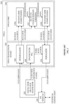
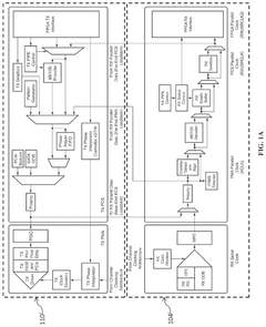
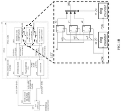
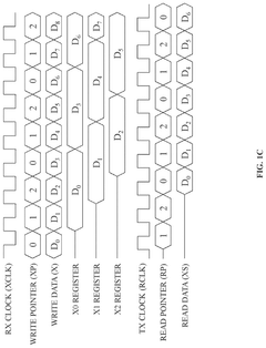
- A field programmable gate array system with an external phase controller that provides phase matching between the receiver and transmitter clocks, using a deserializer and serializer to generate aligned clock signals and a phase control circuit to adjust the transmitter side clock signal based on phase differences, eliminating the need for clock domain crossing circuits that introduce latency.
Hardware Design Standards and Timing Requirements
Hardware design standards for frequency-locked loop (FLL) and FPGA-based systems establish fundamental requirements that directly impact implementation speed and system performance. Industry standards such as IEEE 1076 for VHDL and IEEE 1800 for SystemVerilog define the design methodologies, while timing closure requirements mandate specific propagation delay limits and setup/hold time margins that must be met during implementation.
For FLL systems, hardware design standards emphasize analog circuit specifications including phase noise requirements, lock time parameters, and frequency stability metrics. The implementation must comply with electromagnetic compatibility (EMC) standards such as FCC Part 15 and CISPR 22, which dictate shielding requirements and signal integrity measures. These standards typically require lock times within microseconds and phase noise floors below -120 dBc/Hz at 1 kHz offset, directly influencing the complexity of analog components and PCB layout constraints.
FPGA-based implementations must adhere to timing closure standards that define maximum allowable clock skew, typically less than 10% of the clock period, and setup/hold margins of at least 100 picoseconds. Design rule checks (DRC) and electrical rule checks (ERC) must pass according to foundry-specific guidelines, ensuring signal integrity across high-speed differential pairs and power distribution networks.
Timing requirements for FLL systems center on loop bandwidth specifications, typically ranging from 1 Hz to 10 kHz depending on application requirements. The phase detector sensitivity must meet minimum standards of 1V/radian, while voltage-controlled oscillator gain specifications require linearity within ±5% across the operating frequency range. These parameters directly determine the analog circuit complexity and component selection criteria.
FPGA timing requirements focus on clock domain crossing protocols, requiring proper synchronization circuits and metastability resolution within two clock cycles. Critical path timing must maintain positive slack margins of at least 500 picoseconds to account for process, voltage, and temperature variations. Multi-rate clock systems must implement proper clock gating and enable strategies to minimize power consumption while maintaining timing integrity.
Power delivery network standards mandate voltage ripple specifications below 50 mV peak-to-peak for analog FLL circuits, while FPGA core voltages must maintain regulation within ±3% across all operating conditions. Thermal management requirements specify maximum junction temperatures of 85°C for commercial applications, influencing package selection and heat dissipation strategies that affect overall implementation complexity and development timelines.
Power Efficiency vs Speed Trade-offs Analysis
The fundamental trade-off between power efficiency and implementation speed represents a critical design consideration when comparing Frequency-Locked Loop (FLL) and FPGA-based systems. This analysis reveals distinct performance characteristics that directly impact system architecture decisions across various application domains.
FLL systems demonstrate superior power efficiency through their analog-centric design philosophy. The continuous-time operation of phase detectors, loop filters, and voltage-controlled oscillators inherently consumes less power compared to digital processing alternatives. Typical FLL implementations achieve power consumption levels ranging from 10-50 milliwatts, making them particularly attractive for battery-powered applications and embedded systems with stringent energy constraints.
However, this power advantage comes at the expense of implementation speed flexibility. FLL systems exhibit fixed processing latencies determined by their analog component characteristics and loop dynamics. The settling time for frequency acquisition typically ranges from microseconds to milliseconds, depending on loop bandwidth and reference frequency stability. Once locked, FLLs maintain excellent steady-state performance but struggle with rapid frequency transitions or dynamic reconfiguration requirements.
FPGA-based systems present a contrasting profile, offering exceptional implementation speed capabilities through parallel processing architectures. Modern FPGAs can execute frequency tracking algorithms at clock rates exceeding 500 MHz, enabling sub-microsecond response times for frequency detection and correction. The programmable nature allows for adaptive algorithms that can optimize speed performance based on real-time system conditions.
The power efficiency challenge in FPGA implementations stems from their digital processing overhead. High-speed clock domains, extensive logic resources, and memory interfaces contribute to power consumption levels typically ranging from 100 milliwatts to several watts. Advanced power management techniques, including clock gating, voltage scaling, and selective resource activation, can mitigate these concerns but rarely achieve the inherent efficiency of analog FLL designs.
Application-specific considerations further influence this trade-off analysis. Communications systems requiring rapid channel switching favor FPGA implementations despite higher power consumption, while sensor networks and IoT devices prioritize FLL solutions for extended battery life. The emergence of hybrid architectures combining analog FLL cores with digital control interfaces represents a promising approach to optimize both power efficiency and speed performance simultaneously.
Unlock deeper insights with PatSnap Eureka Quick Research — get a full tech report to explore trends and direct your research. Try now!
Generate Your Research Report Instantly with AI Agent
Supercharge your innovation with PatSnap Eureka AI Agent Platform!