
HBM Memory vs SRAM: Which Provides Higher Data Transfer Rates?
MAY 18, 20268 MIN READ
Generate Your Research Report Instantly with AI Agent
Patsnap Eureka helps you evaluate technical feasibility & market potential.
HBM vs SRAM Memory Technology Background and Performance Goals
The evolution of memory technologies has been fundamentally driven by the relentless demand for higher performance computing systems, particularly in data-intensive applications such as artificial intelligence, high-performance computing, and graphics processing. Two distinct memory architectures have emerged as critical solutions addressing different performance requirements: High Bandwidth Memory (HBM) and Static Random Access Memory (SRAM).
HBM technology represents a revolutionary approach to memory design, originating from the collaborative efforts of major semiconductor manufacturers in the early 2010s. This technology emerged as a response to the bandwidth limitations of traditional memory interfaces, utilizing through-silicon via (TSV) technology and 3D stacking to achieve unprecedented data transfer rates. The development trajectory of HBM has progressed through multiple generations, with each iteration delivering substantial improvements in bandwidth density and energy efficiency.
SRAM technology, conversely, has maintained its position as the gold standard for high-speed, low-latency memory applications since its inception in the 1960s. Built on flip-flop circuits that retain data without refresh cycles, SRAM has continuously evolved through advanced semiconductor process nodes, achieving remarkable improvements in speed and power efficiency while maintaining its fundamental architectural advantages.
The primary performance goal driving HBM development centers on maximizing aggregate bandwidth through parallel data channels. HBM achieves this through wide memory interfaces, typically 1024 bits or more, combined with moderate clock frequencies to deliver exceptional throughput for bandwidth-intensive workloads. This architecture specifically targets applications requiring massive data movement, such as neural network training and scientific simulations.
SRAM's performance objectives focus on minimizing access latency and maximizing random access speed. The technology aims to provide near-instantaneous data retrieval with access times measured in nanoseconds, making it ideal for cache memories and buffer applications where response time is paramount. SRAM's design philosophy prioritizes speed over density, accepting higher cost per bit to achieve superior performance characteristics.
The convergence of these technologies addresses complementary aspects of the memory hierarchy, with each targeting specific performance bottlenecks in modern computing systems. While HBM excels in scenarios demanding high aggregate throughput, SRAM dominates applications requiring ultra-low latency access patterns.
HBM technology represents a revolutionary approach to memory design, originating from the collaborative efforts of major semiconductor manufacturers in the early 2010s. This technology emerged as a response to the bandwidth limitations of traditional memory interfaces, utilizing through-silicon via (TSV) technology and 3D stacking to achieve unprecedented data transfer rates. The development trajectory of HBM has progressed through multiple generations, with each iteration delivering substantial improvements in bandwidth density and energy efficiency.
SRAM technology, conversely, has maintained its position as the gold standard for high-speed, low-latency memory applications since its inception in the 1960s. Built on flip-flop circuits that retain data without refresh cycles, SRAM has continuously evolved through advanced semiconductor process nodes, achieving remarkable improvements in speed and power efficiency while maintaining its fundamental architectural advantages.
The primary performance goal driving HBM development centers on maximizing aggregate bandwidth through parallel data channels. HBM achieves this through wide memory interfaces, typically 1024 bits or more, combined with moderate clock frequencies to deliver exceptional throughput for bandwidth-intensive workloads. This architecture specifically targets applications requiring massive data movement, such as neural network training and scientific simulations.
SRAM's performance objectives focus on minimizing access latency and maximizing random access speed. The technology aims to provide near-instantaneous data retrieval with access times measured in nanoseconds, making it ideal for cache memories and buffer applications where response time is paramount. SRAM's design philosophy prioritizes speed over density, accepting higher cost per bit to achieve superior performance characteristics.
The convergence of these technologies addresses complementary aspects of the memory hierarchy, with each targeting specific performance bottlenecks in modern computing systems. While HBM excels in scenarios demanding high aggregate throughput, SRAM dominates applications requiring ultra-low latency access patterns.
Market Demand for High-Speed Memory Solutions
The global semiconductor industry is experiencing unprecedented demand for high-speed memory solutions, driven by the exponential growth of data-intensive applications across multiple sectors. Artificial intelligence and machine learning workloads require massive parallel processing capabilities, creating substantial pressure on memory subsystems to deliver both high bandwidth and low latency. Graphics processing units, high-performance computing clusters, and data center accelerators represent the primary consumption segments for advanced memory technologies.
Cloud computing infrastructure continues to expand rapidly, with hyperscale data centers demanding memory solutions that can handle increasingly complex workloads. The proliferation of real-time analytics, autonomous vehicles, and edge computing applications has intensified the need for memory architectures capable of supporting sustained high-throughput operations. Traditional memory hierarchies are being challenged by applications that require simultaneous access to large datasets with minimal processing delays.
Enterprise applications spanning financial trading systems, scientific computing, and telecommunications infrastructure are driving specific requirements for memory performance characteristics. High-frequency trading platforms demand ultra-low latency memory access patterns, while scientific simulations require sustained bandwidth for large-scale computational models. The telecommunications sector's transition to advanced network protocols and real-time processing creates additional demand for specialized memory solutions.
Consumer electronics markets are also contributing to high-speed memory demand through gaming applications, virtual reality systems, and mobile devices with enhanced computational capabilities. Gaming platforms increasingly require memory solutions that can support complex graphics rendering and real-time physics calculations. Mobile processors are incorporating more sophisticated AI processing units that benefit from higher memory bandwidth availability.
The automotive industry's shift toward autonomous driving systems represents an emerging market segment with stringent memory performance requirements. Advanced driver assistance systems and autonomous vehicle platforms require real-time processing of sensor data streams, creating demand for memory solutions that can maintain consistent performance under varying operational conditions. These applications often require memory architectures that can balance power efficiency with high-speed data access capabilities.
Manufacturing and industrial automation sectors are adopting more sophisticated control systems that rely on real-time data processing and machine learning algorithms. These applications create demand for memory solutions that can support both deterministic response times and high aggregate throughput for sensor data processing and control loop operations.
Cloud computing infrastructure continues to expand rapidly, with hyperscale data centers demanding memory solutions that can handle increasingly complex workloads. The proliferation of real-time analytics, autonomous vehicles, and edge computing applications has intensified the need for memory architectures capable of supporting sustained high-throughput operations. Traditional memory hierarchies are being challenged by applications that require simultaneous access to large datasets with minimal processing delays.
Enterprise applications spanning financial trading systems, scientific computing, and telecommunications infrastructure are driving specific requirements for memory performance characteristics. High-frequency trading platforms demand ultra-low latency memory access patterns, while scientific simulations require sustained bandwidth for large-scale computational models. The telecommunications sector's transition to advanced network protocols and real-time processing creates additional demand for specialized memory solutions.
Consumer electronics markets are also contributing to high-speed memory demand through gaming applications, virtual reality systems, and mobile devices with enhanced computational capabilities. Gaming platforms increasingly require memory solutions that can support complex graphics rendering and real-time physics calculations. Mobile processors are incorporating more sophisticated AI processing units that benefit from higher memory bandwidth availability.
The automotive industry's shift toward autonomous driving systems represents an emerging market segment with stringent memory performance requirements. Advanced driver assistance systems and autonomous vehicle platforms require real-time processing of sensor data streams, creating demand for memory solutions that can maintain consistent performance under varying operational conditions. These applications often require memory architectures that can balance power efficiency with high-speed data access capabilities.
Manufacturing and industrial automation sectors are adopting more sophisticated control systems that rely on real-time data processing and machine learning algorithms. These applications create demand for memory solutions that can support both deterministic response times and high aggregate throughput for sensor data processing and control loop operations.
Current State and Challenges of HBM and SRAM Technologies
High Bandwidth Memory (HBM) technology has reached its fourth generation, with HBM3 delivering theoretical bandwidth up to 819 GB/s per stack through advanced 3D stacking architecture. Current HBM implementations utilize Through-Silicon Via (TSV) technology to achieve vertical interconnections between memory dies, enabling significantly higher density compared to traditional memory solutions. Leading manufacturers including Samsung, SK Hynix, and Micron have successfully commercialized HBM3 products, with HBM3E variants pushing bandwidth capabilities beyond 1 TB/s per stack.
Static Random Access Memory (SRAM) continues to dominate high-speed cache applications, with modern implementations achieving access times as low as 0.5 nanoseconds in advanced process nodes. Current SRAM technology leverages FinFET transistor structures in 7nm and 5nm processes, enabling higher transistor density while maintaining superior speed characteristics. However, SRAM faces fundamental scaling challenges as transistor dimensions approach physical limits, leading to increased leakage currents and power consumption issues.
The primary challenge facing HBM technology lies in thermal management and power delivery. High-density 3D stacking generates significant heat concentration, requiring sophisticated cooling solutions and limiting sustained performance. Additionally, the complex manufacturing process involving die bonding and TSV formation results in lower yields and higher production costs compared to conventional memory technologies.
SRAM technology confronts scalability limitations as Moore's Law approaches its physical boundaries. Variability in transistor characteristics becomes more pronounced at smaller geometries, affecting memory cell stability and requiring larger design margins. Power consumption has emerged as a critical constraint, particularly in mobile and edge computing applications where energy efficiency is paramount.
Both technologies face integration challenges in heterogeneous computing environments. HBM requires specialized packaging and thermal interface materials, while SRAM must balance speed requirements with power constraints in multi-level cache hierarchies. Manufacturing complexity continues to drive costs higher for both technologies, necessitating careful consideration of performance-per-dollar metrics in commercial applications.
Static Random Access Memory (SRAM) continues to dominate high-speed cache applications, with modern implementations achieving access times as low as 0.5 nanoseconds in advanced process nodes. Current SRAM technology leverages FinFET transistor structures in 7nm and 5nm processes, enabling higher transistor density while maintaining superior speed characteristics. However, SRAM faces fundamental scaling challenges as transistor dimensions approach physical limits, leading to increased leakage currents and power consumption issues.
The primary challenge facing HBM technology lies in thermal management and power delivery. High-density 3D stacking generates significant heat concentration, requiring sophisticated cooling solutions and limiting sustained performance. Additionally, the complex manufacturing process involving die bonding and TSV formation results in lower yields and higher production costs compared to conventional memory technologies.
SRAM technology confronts scalability limitations as Moore's Law approaches its physical boundaries. Variability in transistor characteristics becomes more pronounced at smaller geometries, affecting memory cell stability and requiring larger design margins. Power consumption has emerged as a critical constraint, particularly in mobile and edge computing applications where energy efficiency is paramount.
Both technologies face integration challenges in heterogeneous computing environments. HBM requires specialized packaging and thermal interface materials, while SRAM must balance speed requirements with power constraints in multi-level cache hierarchies. Manufacturing complexity continues to drive costs higher for both technologies, necessitating careful consideration of performance-per-dollar metrics in commercial applications.
Current Memory Solutions for Data Transfer Rate Optimization
01 High-bandwidth memory interface optimization
Technologies for optimizing high-bandwidth memory interfaces focus on improving data transfer rates through enhanced signaling protocols, advanced memory controllers, and optimized bus architectures. These solutions address bandwidth limitations and latency issues in high-performance computing applications by implementing sophisticated memory management techniques and interface designs.- High-bandwidth memory interface optimization techniques: Advanced interface optimization methods focus on improving data throughput between high-bandwidth memory systems and processing units. These techniques involve sophisticated signaling protocols, enhanced data path architectures, and optimized timing mechanisms to maximize transfer efficiency. The implementations include multi-channel configurations and parallel data streaming capabilities that significantly boost overall system performance.
- SRAM cache memory access acceleration: Specialized methods for enhancing static random-access memory performance through improved access patterns and reduced latency mechanisms. These approaches utilize advanced addressing schemes, predictive caching algorithms, and optimized read/write operations to minimize access time. The techniques also incorporate intelligent prefetching and data organization strategies to maintain high-speed data availability.
- Memory controller architecture for enhanced data flow: Innovative controller designs that manage data transfer operations between different memory types and system components. These architectures implement sophisticated scheduling algorithms, buffer management systems, and priority-based data handling to optimize throughput. The controllers feature adaptive bandwidth allocation and dynamic performance tuning capabilities to respond to varying workload demands.
- Multi-level memory hierarchy optimization: Comprehensive strategies for coordinating data movement across multiple memory levels including cache, main memory, and storage systems. These methods employ intelligent data placement algorithms, coherency protocols, and performance monitoring to ensure optimal data locality. The implementations feature automated tier management and adaptive caching policies that respond to application access patterns.
- Power-efficient memory transfer protocols: Energy-conscious approaches to memory data transfer that balance performance requirements with power consumption constraints. These protocols implement dynamic voltage scaling, selective activation of memory banks, and intelligent power gating mechanisms. The methods also incorporate thermal management considerations and adaptive frequency scaling to maintain optimal power efficiency during high-speed data operations.
02 SRAM cache memory data transfer enhancement
Methods for enhancing data transfer rates in SRAM-based cache systems involve optimizing memory access patterns, implementing advanced prefetching algorithms, and utilizing multi-port memory architectures. These approaches focus on reducing access latency and increasing throughput through improved memory organization and control mechanisms.Expand Specific Solutions03 Memory controller and arbitration systems
Advanced memory controller designs and arbitration systems manage data flow between different memory types and processing units. These systems implement sophisticated scheduling algorithms, priority management, and bandwidth allocation techniques to optimize overall system performance and ensure efficient utilization of available memory resources.Expand Specific Solutions04 Multi-level memory hierarchy optimization
Techniques for optimizing multi-level memory hierarchies involve coordinating data movement between different memory tiers, implementing intelligent caching strategies, and managing data placement policies. These solutions aim to maximize the benefits of both high-speed SRAM and high-capacity memory technologies through efficient data migration and access prediction.Expand Specific Solutions05 Memory interface timing and synchronization
Advanced timing and synchronization mechanisms for memory interfaces address clock domain crossing, signal integrity, and data coherency challenges. These technologies implement precise timing control, error correction, and synchronization protocols to maintain data integrity while maximizing transfer rates across different memory subsystems.Expand Specific Solutions
Key Players in HBM and SRAM Memory Industry
The HBM memory versus SRAM data transfer rate competition represents a mature technology landscape in the growth phase, with the global high-bandwidth memory market expanding rapidly driven by AI and data center demands. While SRAM traditionally offers superior speed for cache applications, HBM technology has achieved significant breakthroughs in bandwidth capabilities. Major players demonstrate varying technological maturity levels: Samsung Electronics, Micron Technology, and Intel lead in HBM production with advanced manufacturing capabilities, while AMD and IBM excel in system integration. Asian manufacturers like ChangXin Memory Technologies and Taiwan Semiconductor Manufacturing represent emerging competitive forces. Research institutions including Zhejiang University contribute to next-generation memory architectures, while specialized companies like AvicenaTech focus on optical interconnect solutions to overcome traditional memory bandwidth limitations.
Advanced Micro Devices, Inc.
Technical Solution: AMD integrates HBM technology in their high-performance computing and graphics solutions, achieving memory bandwidth up to 2,048 GB/s in their MI300 series accelerators through quad-HBM3 configurations. AMD's strategy emphasizes maximizing HBM's bandwidth advantages while mitigating latency concerns through advanced memory scheduling algorithms and large on-chip cache hierarchies. Their Infinity Cache technology works in conjunction with HBM to provide a balanced memory subsystem that can deliver both high throughput and reasonable access latency. AMD also implements sophisticated power management techniques to optimize the power-performance trade-offs between HBM and SRAM usage patterns.
Strengths: Excellent bandwidth scaling, innovative cache integration, competitive power efficiency. Weaknesses: Limited SRAM capacity for ultra-low latency needs, complex memory hierarchy management, cost considerations for mainstream applications.
Samsung Electronics Co., Ltd.
Technical Solution: Samsung has developed advanced HBM3E technology achieving data transfer rates up to 1,280 GB/s per stack with 9.8 Gbps per pin speed. Their HBM solutions utilize through-silicon via (TSV) technology and advanced packaging techniques to stack multiple DRAM dies vertically, enabling massive parallel data access. Samsung's HBM memory provides significantly higher bandwidth compared to traditional SRAM by leveraging wide I/O interfaces with thousands of data pins operating simultaneously. The company has also implemented advanced thermal management and power delivery systems to maintain performance stability under high-speed operations.
Strengths: Industry-leading HBM bandwidth, mature manufacturing process, excellent thermal management. Weaknesses: Higher latency compared to SRAM, more complex packaging requirements, higher power consumption per bit.
Core Innovations in HBM and SRAM Transfer Technologies
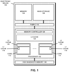
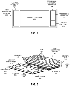
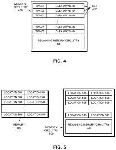
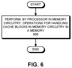
Performing Operations for Handling Data using Processor in Memory Circuitry in a High Bandwidth Memory
PatentInactiveUS20230359556A1
Innovation
- Implementing processor in memory (PIM) circuitry within high bandwidth memory to perform cache operations and handle data, reducing the need for processors to handle these tasks directly, thereby offloading operations and improving performance.
Interconnection structures for high bandwidth data transfer
PatentActiveUS12119335B2
Innovation
- The implementation of high bandwidth semiconductor chips and modules with companion PHYs connected to SERDES, enabling serial communication links that extend communication distances and allow for denser packing of HBMs around central dies, using a combination of parallel and serial interfaces and distant I/O connections.


Power Efficiency Trade-offs in Memory Architecture Design
Power consumption represents a critical design consideration when comparing HBM memory and SRAM architectures, as each technology exhibits distinct energy characteristics that significantly impact overall system performance and operational costs. The fundamental differences in their underlying technologies create inherent trade-offs between power efficiency and data transfer capabilities.
HBM memory demonstrates superior power efficiency per bit compared to SRAM due to its DRAM-based architecture and advanced packaging techniques. The 3D stacking approach in HBM reduces the physical distance between memory dies and the processor, minimizing power losses associated with signal transmission. Additionally, HBM operates at lower voltages, typically around 1.2V, compared to SRAM's higher voltage requirements, resulting in reduced static power consumption across large memory arrays.
SRAM architectures, while offering exceptional speed performance, consume significantly more power per bit stored. The six-transistor cell structure required for each SRAM bit creates substantial static leakage currents, particularly as manufacturing processes scale down to smaller geometries. This leakage power becomes increasingly problematic in large cache implementations, where millions of SRAM cells must maintain their state continuously.
The power efficiency equation becomes more complex when considering dynamic power consumption during active data transfers. HBM's wide parallel interface distributes power consumption across multiple channels, enabling high bandwidth while maintaining reasonable power density. However, the refresh requirements inherent to DRAM technology introduce periodic power spikes that SRAM architectures avoid entirely.
Thermal management considerations further complicate power efficiency trade-offs. SRAM's concentrated power dissipation in smaller areas can create hotspots that require sophisticated cooling solutions, potentially offsetting some of the raw performance advantages. HBM's distributed heat generation across stacked dies presents different thermal challenges but generally offers more manageable power density profiles.
Modern memory controllers increasingly implement dynamic power management techniques, including selective bank activation and adaptive voltage scaling, to optimize power efficiency based on workload characteristics. These innovations help bridge the power efficiency gap between HBM and SRAM implementations, though fundamental architectural differences continue to influence optimal application scenarios.
HBM memory demonstrates superior power efficiency per bit compared to SRAM due to its DRAM-based architecture and advanced packaging techniques. The 3D stacking approach in HBM reduces the physical distance between memory dies and the processor, minimizing power losses associated with signal transmission. Additionally, HBM operates at lower voltages, typically around 1.2V, compared to SRAM's higher voltage requirements, resulting in reduced static power consumption across large memory arrays.
SRAM architectures, while offering exceptional speed performance, consume significantly more power per bit stored. The six-transistor cell structure required for each SRAM bit creates substantial static leakage currents, particularly as manufacturing processes scale down to smaller geometries. This leakage power becomes increasingly problematic in large cache implementations, where millions of SRAM cells must maintain their state continuously.
The power efficiency equation becomes more complex when considering dynamic power consumption during active data transfers. HBM's wide parallel interface distributes power consumption across multiple channels, enabling high bandwidth while maintaining reasonable power density. However, the refresh requirements inherent to DRAM technology introduce periodic power spikes that SRAM architectures avoid entirely.
Thermal management considerations further complicate power efficiency trade-offs. SRAM's concentrated power dissipation in smaller areas can create hotspots that require sophisticated cooling solutions, potentially offsetting some of the raw performance advantages. HBM's distributed heat generation across stacked dies presents different thermal challenges but generally offers more manageable power density profiles.
Modern memory controllers increasingly implement dynamic power management techniques, including selective bank activation and adaptive voltage scaling, to optimize power efficiency based on workload characteristics. These innovations help bridge the power efficiency gap between HBM and SRAM implementations, though fundamental architectural differences continue to influence optimal application scenarios.
Cost-Performance Analysis of Advanced Memory Technologies
The cost-performance analysis of HBM memory versus SRAM reveals significant trade-offs that organizations must carefully evaluate when selecting memory technologies for high-performance computing applications. While SRAM traditionally offers superior data transfer rates, the economic implications of implementing either technology vary substantially across different use cases and deployment scales.
From a pure performance perspective, SRAM maintains its advantage in raw data transfer speeds, typically achieving access times of 1-2 nanoseconds compared to HBM's 10-15 nanoseconds. However, the cost differential between these technologies creates a complex optimization challenge. SRAM manufacturing costs remain approximately 10-15 times higher per gigabyte than HBM, primarily due to the six-transistor cell structure requiring significantly more silicon area per bit stored.
The economic analysis becomes more nuanced when considering total cost of ownership. HBM's higher density allows for reduced system complexity, fewer memory controllers, and lower power consumption per bit accessed. These factors contribute to substantial savings in infrastructure costs, particularly in data center environments where power efficiency directly impacts operational expenses. The 3D stacking architecture of HBM enables memory densities exceeding 24GB per stack, while SRAM implementations typically require distributed cache hierarchies to achieve comparable effective capacity.
Performance-per-dollar metrics favor HBM in applications requiring large memory footprints with moderate access frequency. The bandwidth efficiency of HBM, reaching up to 1.2TB/s per stack, provides exceptional throughput for streaming applications and large dataset processing. Conversely, SRAM's cost-performance advantage emerges in scenarios demanding ultra-low latency access to smaller datasets, such as processor caches and real-time control systems.
Manufacturing scalability further influences the cost-performance equation. HBM production benefits from established DRAM fabrication processes and economies of scale, while SRAM manufacturing faces inherent limitations in density scaling. As process nodes advance, the relative cost advantage of HBM is expected to increase, making it increasingly attractive for applications previously dominated by SRAM implementations.
From a pure performance perspective, SRAM maintains its advantage in raw data transfer speeds, typically achieving access times of 1-2 nanoseconds compared to HBM's 10-15 nanoseconds. However, the cost differential between these technologies creates a complex optimization challenge. SRAM manufacturing costs remain approximately 10-15 times higher per gigabyte than HBM, primarily due to the six-transistor cell structure requiring significantly more silicon area per bit stored.
The economic analysis becomes more nuanced when considering total cost of ownership. HBM's higher density allows for reduced system complexity, fewer memory controllers, and lower power consumption per bit accessed. These factors contribute to substantial savings in infrastructure costs, particularly in data center environments where power efficiency directly impacts operational expenses. The 3D stacking architecture of HBM enables memory densities exceeding 24GB per stack, while SRAM implementations typically require distributed cache hierarchies to achieve comparable effective capacity.
Performance-per-dollar metrics favor HBM in applications requiring large memory footprints with moderate access frequency. The bandwidth efficiency of HBM, reaching up to 1.2TB/s per stack, provides exceptional throughput for streaming applications and large dataset processing. Conversely, SRAM's cost-performance advantage emerges in scenarios demanding ultra-low latency access to smaller datasets, such as processor caches and real-time control systems.
Manufacturing scalability further influences the cost-performance equation. HBM production benefits from established DRAM fabrication processes and economies of scale, while SRAM manufacturing faces inherent limitations in density scaling. As process nodes advance, the relative cost advantage of HBM is expected to increase, making it increasingly attractive for applications previously dominated by SRAM implementations.
Unlock deeper insights with Patsnap Eureka Quick Research — get a full tech report to explore trends and direct your research. Try now!
Generate Your Research Report Instantly with AI Agent
Supercharge your innovation with Patsnap Eureka AI Agent Platform!