

How to Reduce Latency in HBM Memory Systems
MAY 18, 20268 MIN READ
Generate Your Research Report Instantly with AI Agent
PatSnap Eureka helps you evaluate technical feasibility & market potential.
HBM Memory Latency Challenges and Performance Goals
High Bandwidth Memory (HBM) technology has emerged as a critical solution for addressing the growing memory bandwidth demands of modern computing applications, particularly in high-performance computing, artificial intelligence, and graphics processing. Since its introduction in 2013, HBM has undergone significant evolution through multiple generations, with each iteration focusing on increasing bandwidth while simultaneously addressing latency concerns that have become increasingly prominent as applications demand both high throughput and low response times.
The evolution of HBM technology demonstrates a clear trajectory toward enhanced performance metrics. HBM1 initially provided 128 GB/s bandwidth per stack, while HBM2 expanded this to 307 GB/s, and the latest HBM3 specifications target up to 819 GB/s. However, this bandwidth-focused development has revealed that raw throughput alone is insufficient for many contemporary applications, particularly those involving real-time processing, interactive workloads, and latency-sensitive computational tasks.
Current latency challenges in HBM systems stem from multiple architectural factors. The 3D stacked architecture, while enabling high bandwidth through wide interfaces, introduces additional signal propagation delays through the vertical interconnects. The through-silicon vias (TSVs) that enable inter-die communication add parasitic capacitance and resistance, contributing to signal integrity issues and increased access times. Memory controller complexity has also grown substantially to manage the wide data paths and multiple channels, introducing additional processing overhead.
Performance goals for next-generation HBM systems increasingly emphasize balanced optimization between bandwidth and latency. Target specifications aim for sub-100 nanosecond access latencies while maintaining the high bandwidth capabilities that define HBM technology. These objectives require addressing both the physical layer constraints inherent in 3D stacking and the protocol-level inefficiencies in current memory access patterns.
The industry recognizes that achieving these performance goals necessitates fundamental innovations across multiple domains. Physical design improvements must address signal integrity and propagation delays, while architectural enhancements should focus on reducing protocol overhead and optimizing data access patterns. Advanced error correction mechanisms that minimize latency penalties and intelligent prefetching strategies represent additional areas where significant improvements are expected to emerge in future HBM generations.
Market Demand for Low-Latency HBM Solutions
The demand for low-latency HBM memory solutions is experiencing unprecedented growth across multiple high-performance computing sectors. Data centers and cloud service providers represent the largest market segment, driven by the exponential increase in artificial intelligence workloads and machine learning applications that require rapid data access patterns. These environments demand memory systems capable of handling massive parallel processing tasks with minimal delay, making latency reduction a critical performance differentiator.
High-performance computing applications in scientific research, financial modeling, and simulation environments constitute another significant demand driver. These applications often involve complex computational workflows where memory access bottlenecks can severely impact overall system performance. Research institutions and enterprises are increasingly prioritizing memory systems that can deliver consistent low-latency performance under sustained high-bandwidth conditions.
The gaming and graphics processing market has emerged as a substantial consumer of low-latency HBM solutions. Advanced graphics cards and gaming systems require memory architectures that can support real-time rendering, virtual reality applications, and high-resolution gaming experiences. The growing popularity of esports and professional gaming has intensified the focus on minimizing input lag and rendering delays.
Automotive and autonomous vehicle development represents a rapidly expanding market segment with stringent latency requirements. Advanced driver assistance systems and autonomous driving platforms demand real-time processing capabilities where memory access delays can have safety-critical implications. The automotive industry's transition toward software-defined vehicles is creating sustained demand for high-performance memory solutions.
Edge computing and Internet of Things applications are driving demand for compact, energy-efficient HBM solutions with optimized latency characteristics. These applications require memory systems that can deliver consistent performance in resource-constrained environments while maintaining low power consumption profiles.
The telecommunications sector, particularly with the deployment of advanced network infrastructure and edge computing nodes, requires memory solutions that can handle high-frequency data processing with minimal latency. Network function virtualization and software-defined networking applications depend heavily on memory performance characteristics to maintain service quality and responsiveness.
Market growth is further accelerated by the increasing adoption of artificial intelligence accelerators and specialized processing units that rely on HBM memory architectures to achieve optimal performance in machine learning inference and training workloads.
Current HBM Latency Bottlenecks and Technical Barriers
High Bandwidth Memory systems face several critical latency bottlenecks that significantly impact overall system performance. The most prominent bottleneck stems from the inherent architectural limitations of the Through-Silicon Via technology used in HBM stacks. TSV interconnects, while enabling vertical integration, introduce parasitic capacitance and resistance that create signal propagation delays between memory dies. These delays become more pronounced as stack heights increase, with each additional die layer contributing cumulative latency overhead.
Memory controller arbitration represents another substantial bottleneck in HBM systems. The complex scheduling algorithms required to manage multiple memory channels and maintain data coherency across the wide interface create processing delays. Current controllers must handle up to 1024-bit wide data paths while coordinating access patterns across multiple pseudo-channels, leading to increased decision-making latency that directly impacts memory response times.
Thermal management constraints pose significant technical barriers to latency reduction efforts. HBM stacks generate concentrated heat due to their high-density architecture, necessitating thermal throttling mechanisms that deliberately reduce operating frequencies to prevent overheating. This thermal limitation creates a fundamental trade-off between performance and reliability, as higher speeds that could reduce latency are constrained by temperature thresholds.
Signal integrity challenges across the wide HBM interface create additional latency barriers. The extensive parallel data paths are susceptible to crosstalk, power delivery noise, and timing skew issues that require error correction mechanisms and conservative timing margins. These protective measures, while necessary for reliable operation, introduce additional processing cycles that increase overall memory access latency.
Bank conflict resolution mechanisms represent another critical bottleneck area. HBM systems must manage simultaneous access requests across multiple banks and channels, requiring sophisticated conflict detection and resolution protocols. When multiple requests target the same bank or violate timing constraints, the memory controller must serialize these operations, creating wait states that directly translate to increased latency.
The physical limitations of DRAM cell refresh operations create unavoidable latency penalties in HBM systems. The high-density nature of HBM requires frequent refresh cycles to maintain data integrity, during which targeted banks become temporarily unavailable for normal operations. These refresh-induced delays are particularly problematic in latency-sensitive applications where predictable memory response times are crucial for optimal system performance.
Existing HBM Latency Optimization Techniques
01 Memory access scheduling and arbitration techniques
Advanced scheduling algorithms and arbitration mechanisms are employed to optimize memory access patterns and reduce latency in high bandwidth memory systems. These techniques involve intelligent request queuing, priority-based access control, and dynamic scheduling to minimize wait times and improve overall system performance.- Memory access scheduling and arbitration techniques: Advanced scheduling algorithms and arbitration mechanisms are employed to optimize memory access patterns and reduce latency in high bandwidth memory systems. These techniques involve intelligent request queuing, priority-based access control, and dynamic scheduling to minimize wait times and improve overall system performance.
- Memory controller optimization and buffering strategies: Memory controllers are enhanced with sophisticated buffering mechanisms and optimization techniques to reduce latency. These improvements include advanced buffer management, prefetching strategies, and intelligent caching mechanisms that anticipate memory access patterns and reduce the time required for data retrieval.
- High-speed interface and signaling improvements: Interface design and signaling protocols are optimized to achieve faster data transmission and reduced communication delays. These enhancements focus on improving the physical layer characteristics, signal integrity, and timing optimization to minimize the latency associated with data transfer between memory components and processors.
- Memory architecture and topology optimization: System architecture modifications and memory topology designs are implemented to create more efficient data paths and reduce access latency. These approaches involve optimizing the physical arrangement of memory components, implementing hierarchical memory structures, and designing interconnect architectures that minimize data travel distances and access times.
- Error correction and reliability mechanisms with low latency impact: Error correction codes and reliability mechanisms are designed to maintain data integrity while minimizing their impact on system latency. These solutions implement efficient error detection and correction algorithms that operate with minimal performance overhead, ensuring system reliability without significantly increasing memory access times.
02 Cache optimization and prefetching strategies
Implementation of sophisticated caching mechanisms and predictive prefetching algorithms to reduce memory access latency. These approaches involve multi-level cache hierarchies, intelligent data prediction, and proactive memory loading to ensure frequently accessed data is readily available, thereby minimizing system delays.Expand Specific Solutions03 Memory controller architecture enhancements
Specialized memory controller designs that incorporate advanced buffering, pipelining, and parallel processing capabilities to reduce latency in high bandwidth memory systems. These controllers feature optimized command processing, enhanced data path management, and improved timing control mechanisms.Expand Specific Solutions04 Interface and protocol optimization
Development of enhanced communication protocols and interface standards specifically designed to minimize latency in memory transactions. These optimizations include reduced command overhead, streamlined data transfer mechanisms, and improved synchronization methods between memory components and processing units.Expand Specific Solutions05 Power management and thermal considerations
Integration of intelligent power management techniques and thermal optimization strategies that maintain low latency performance while managing energy consumption and heat generation. These solutions balance performance requirements with power efficiency through dynamic voltage scaling, selective component activation, and thermal-aware operation modes.Expand Specific Solutions
Key Players in HBM Memory and Controller Industry
The HBM memory latency reduction market is in a mature growth stage, driven by increasing demand for high-performance computing and AI applications. The market demonstrates significant scale with established players like Samsung Electronics, Micron Technology, and Intel leading traditional memory manufacturing, while NVIDIA dominates GPU-integrated HBM solutions. Technology maturity varies across segments, with Samsung and Micron achieving advanced HBM3 production capabilities, Intel focusing on processor-memory integration, and emerging players like ChangXin Memory Technologies and Tenstorrent developing specialized AI-optimized solutions. The competitive landscape shows consolidation around proven architectures, though innovation continues in areas like through-silicon vias, advanced packaging, and memory controller optimization, indicating a technologically mature but rapidly evolving market.
Micron Technology, Inc.
Technical Solution: Micron focuses on reducing HBM latency through innovative memory array architectures and advanced process technologies. Their solution incorporates optimized sense amplifier designs and reduced parasitic capacitances to accelerate data access times. The company implements intelligent memory scheduling algorithms within the memory controller that prioritize critical memory requests and minimize bank conflicts. Additionally, Micron utilizes advanced packaging techniques including optimized bump pitch and improved thermal management to maintain consistent low-latency performance under varying operational conditions.
Strengths: Strong focus on memory-specific optimizations with extensive experience in high-performance memory solutions and competitive pricing strategies. Weaknesses: Smaller market share in HBM compared to Samsung and limited vertical integration capabilities with processor manufacturers.
Samsung Electronics Co., Ltd.
Technical Solution: Samsung implements advanced HBM3 technology with optimized memory controller architectures that reduce access latency through improved bank management and intelligent prefetching mechanisms. Their approach includes dynamic voltage and frequency scaling (DVFS) to balance performance and power consumption, along with enhanced Through-Silicon Via (TSV) designs that minimize signal propagation delays. The company also employs sophisticated error correction codes (ECC) that operate with minimal latency overhead while maintaining data integrity across high-speed memory operations.
Strengths: Leading HBM manufacturing capabilities with proven high-volume production experience and strong integration with major GPU vendors. Weaknesses: Higher power consumption compared to some competing solutions and premium pricing for advanced HBM variants.
Core Innovations in HBM Latency Reduction Patents
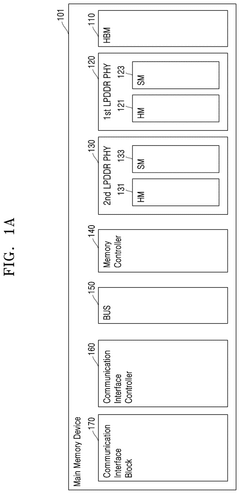
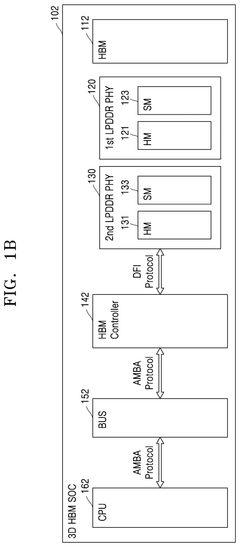
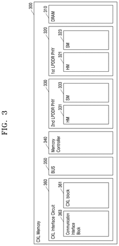
Memory device, CXL memory device, system in package, and system on chip including high bandwidth memory
PatentPendingUS20250103488A1
Innovation
- Incorporating an HBM interface intellectual property (IP) core that directly converts the interface of HBM core devices into the DFI protocol, bypassing the need for JEDEC interface conversion, thereby reducing the number of protocol and interface conversions required.
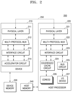
System and method for a high bandwidth-low latency memory controller
PatentInactiveUS6957298B1
Innovation
- A memory controller system with multiple command streams that separates references from computer components, allowing instantaneous switching between streams to hide bank preparation commands, thereby achieving low latency and high bandwidth while preserving bank state.


Power Efficiency Considerations in HBM Design
Power efficiency represents a critical design constraint in HBM memory systems, particularly when implementing latency reduction techniques. The pursuit of lower latency often conflicts with power optimization goals, creating complex engineering trade-offs that require careful consideration throughout the design process.
Dynamic voltage and frequency scaling (DVFS) emerges as a fundamental approach to balance latency and power consumption. By adjusting operating voltages and frequencies based on workload demands, HBM controllers can maintain acceptable latency performance while minimizing power draw during periods of reduced activity. Advanced DVFS implementations utilize predictive algorithms to anticipate memory access patterns and preemptively adjust power states.
The implementation of aggressive prefetching mechanisms, while effective for latency reduction, introduces significant power overhead through speculative memory accesses. Power-aware prefetching strategies must incorporate confidence metrics and access pattern analysis to minimize unnecessary power consumption while preserving latency benefits. Selective prefetching based on application characteristics and thermal constraints provides a viable compromise.
Clock gating and power gating techniques play essential roles in managing power consumption within HBM stacks. Fine-grained clock gating at the bank and sub-bank levels allows inactive memory regions to reduce power consumption without impacting active operations. Power gating strategies must account for wake-up latencies to ensure that power-saving modes do not inadvertently increase overall system latency.
Thermal management considerations directly impact both power efficiency and latency performance in HBM systems. Elevated temperatures increase leakage power while potentially degrading timing margins, necessitating thermal-aware scheduling algorithms that distribute memory accesses across different stack regions to prevent hotspot formation.
Advanced error correction schemes, while necessary for reliability, contribute to both latency and power overhead. Low-power ECC implementations utilizing adaptive correction strength based on error rates and criticality levels help minimize the power impact of reliability features. On-die ECC engines with optimized encoding algorithms reduce the computational power requirements while maintaining correction capabilities.
The integration of near-data processing capabilities within HBM stacks offers opportunities to reduce overall system power consumption by minimizing data movement between memory and processing units. However, these implementations must carefully manage the additional power overhead introduced by processing elements while ensuring that computational tasks do not interfere with memory access latency requirements.
Thermal Management Challenges in HBM Systems
High Bandwidth Memory (HBM) systems face significant thermal management challenges that directly impact latency performance and overall system reliability. The three-dimensional stacking architecture of HBM, while enabling superior bandwidth density, creates concentrated heat generation zones that can severely affect memory access times and data integrity.
The vertical stacking of multiple DRAM dies in HBM modules results in thermal hotspots, particularly in the middle layers where heat dissipation paths are most constrained. These elevated temperatures can cause timing parameter drift, leading to increased access latencies as the memory controller must implement conservative timing margins to ensure data reliability. Temperature variations across different die layers also create non-uniform performance characteristics within a single HBM stack.
Thermal-induced voltage fluctuations represent another critical challenge in HBM systems. As junction temperatures rise, transistor switching characteristics change, potentially causing voltage droops that trigger error correction mechanisms or force the memory to operate at reduced frequencies. This thermal-electrical coupling creates a direct pathway between temperature management and latency performance.
The proximity of HBM stacks to high-performance processors exacerbates thermal challenges. Graphics processing units and central processing units generate substantial heat loads that can elevate ambient temperatures around HBM modules. This thermal coupling between compute and memory subsystems requires coordinated thermal management strategies to prevent cascading performance degradation.
Current thermal management approaches include advanced packaging solutions with integrated heat spreaders, micro-channel cooling systems, and dynamic thermal throttling mechanisms. However, these solutions often involve trade-offs between thermal performance and system complexity. Emerging techniques such as phase-change materials, vapor chamber integration, and intelligent thermal monitoring systems show promise for addressing these challenges while maintaining optimal latency characteristics in next-generation HBM implementations.
Unlock deeper insights with PatSnap Eureka Quick Research — get a full tech report to explore trends and direct your research. Try now!
Generate Your Research Report Instantly with AI Agent
Supercharge your innovation with PatSnap Eureka AI Agent Platform!