

Improvements in Substrate Bonding Through Lithographic Approaches
APR 24, 20269 MIN READ
Generate Your Research Report Instantly with AI Agent
PatSnap Eureka helps you evaluate technical feasibility & market potential.
Lithographic Substrate Bonding Background and Objectives
Substrate bonding has emerged as a critical enabling technology in the semiconductor industry, particularly as device miniaturization and heterogeneous integration demands continue to escalate. Traditional bonding methods, including thermal compression bonding, anodic bonding, and adhesive bonding, have served the industry well for decades but face increasing limitations in meeting the stringent requirements of advanced packaging applications. These conventional approaches often struggle with achieving the precise alignment, uniform bonding strength, and minimal thermal budget required for next-generation devices.
The evolution of substrate bonding technology has been driven by the relentless pursuit of higher device density, improved electrical performance, and enhanced thermal management capabilities. Early bonding techniques relied primarily on mechanical pressure and elevated temperatures to achieve adequate adhesion between substrates. However, as feature sizes shrunk and integration complexity increased, the industry recognized the need for more sophisticated bonding methodologies that could deliver superior precision and reliability.
Lithographic approaches to substrate bonding represent a paradigm shift in how bonding interfaces are designed and implemented. By leveraging the precision and scalability inherent in lithographic processes, these methods enable the creation of highly controlled bonding structures with nanometer-level accuracy. This technological advancement addresses several critical challenges that have historically limited the performance and yield of bonded substrate assemblies.
The primary objective of implementing lithographic approaches in substrate bonding is to achieve unprecedented control over the bonding interface characteristics. This includes precise definition of bonding pad geometries, optimization of surface topography, and creation of specialized bonding structures that enhance mechanical and electrical connectivity. Through photolithographic patterning, manufacturers can define bonding regions with exceptional accuracy, enabling the realization of ultra-fine pitch interconnects that were previously unattainable.
Another fundamental goal is to minimize process-induced stress and thermal exposure during bonding operations. Lithographic methods allow for the pre-definition of bonding materials and structures, reducing the need for high-temperature processing steps that can adversely affect device performance. This approach is particularly crucial for temperature-sensitive components and heterogeneous integration scenarios where different materials with varying thermal expansion coefficients must be reliably bonded.
The strategic importance of lithographic substrate bonding extends beyond immediate technical benefits to encompass broader manufacturing and economic advantages. By enabling more predictable and repeatable bonding processes, these approaches contribute to improved yield rates and reduced manufacturing costs, making advanced packaging solutions more commercially viable for a wider range of applications.
Market Demand for Advanced Substrate Bonding Solutions
The semiconductor industry's relentless pursuit of miniaturization and performance enhancement has created unprecedented demand for advanced substrate bonding solutions. As device architectures evolve toward three-dimensional integration and heterogeneous packaging, traditional bonding methods face significant limitations in achieving the precision and reliability required for next-generation applications. This technological gap has intensified market interest in lithographic approaches to substrate bonding, which offer superior control over bonding interfaces and enable novel device configurations.
Market drivers for advanced substrate bonding solutions span multiple high-growth sectors. The artificial intelligence and machine learning boom has accelerated demand for high-bandwidth memory solutions and advanced processor architectures that rely on sophisticated substrate bonding techniques. Data centers require increasingly efficient thermal management and electrical performance, pushing the boundaries of conventional bonding technologies. Meanwhile, the automotive industry's transition toward electric vehicles and autonomous driving systems demands robust, high-performance semiconductor solutions that can withstand harsh operating conditions.
Consumer electronics markets continue to drive miniaturization trends, with smartphones, tablets, and wearable devices requiring thinner profiles and enhanced functionality. These applications necessitate advanced packaging solutions that can accommodate multiple die configurations while maintaining electrical performance and thermal efficiency. The integration of sensors, processors, and memory components in compact form factors has become a critical competitive advantage, directly influencing substrate bonding technology adoption.
The telecommunications sector's deployment of fifth-generation networks has created substantial demand for high-frequency, low-loss substrate bonding solutions. Radio frequency applications require precise control over electrical characteristics at bonding interfaces, making lithographic approaches particularly attractive for their ability to create uniform, well-defined bonding regions with minimal parasitic effects.
Emerging applications in quantum computing, photonics, and biomedical devices represent nascent but potentially transformative market segments. These specialized applications often require custom bonding solutions that can accommodate unique material combinations and operating environments, creating opportunities for innovative lithographic bonding approaches.
The market landscape reflects growing recognition that substrate bonding represents a critical bottleneck in advanced semiconductor manufacturing. Industry stakeholders increasingly view bonding technology as a key differentiator rather than a commodity process, driving investment in next-generation solutions that can enable new device architectures and performance levels.
Current Challenges in Lithographic Bonding Technologies
Lithographic bonding technologies face significant technical barriers that limit their widespread adoption in advanced semiconductor manufacturing and heterogeneous integration applications. One of the primary challenges lies in achieving precise alignment between substrates during the bonding process. Current lithographic systems struggle to maintain sub-micron alignment accuracy across large wafer areas, particularly when dealing with thermal expansion mismatches between different substrate materials. This alignment precision becomes increasingly critical as device dimensions shrink and integration density increases.
Surface preparation and cleanliness represent another major obstacle in lithographic bonding processes. Contaminants, particles, and surface roughness can severely compromise bond quality and yield. Traditional cleaning methods often prove insufficient for the stringent requirements of lithographic bonding, where even nanoscale impurities can create defects that propagate throughout the bonded structure. The challenge is compounded when working with diverse substrate materials that require different surface treatment protocols.
Temperature control during the lithographic bonding process presents complex engineering challenges. Maintaining uniform temperature distribution across large substrate areas while preventing thermal stress-induced deformation requires sophisticated heating systems and real-time monitoring capabilities. The thermal budget constraints of pre-existing device structures further complicate the process, as excessive temperatures can damage sensitive components or alter material properties.
Interface chemistry and adhesion mechanisms pose fundamental scientific challenges in lithographic bonding. Understanding and controlling the molecular-level interactions between different substrate materials remains an active area of research. The formation of reliable chemical bonds while avoiding unwanted interfacial reactions requires precise control of surface chemistry, ambient conditions, and processing parameters.
Process throughput and scalability issues significantly impact the commercial viability of lithographic bonding technologies. Current systems often require extended processing times and complex multi-step procedures that limit manufacturing efficiency. The need for specialized equipment and controlled environments adds substantial cost and complexity to production workflows.
Defect detection and quality control present ongoing challenges due to the buried nature of bonded interfaces. Traditional inspection methods may not adequately identify subsurface defects or weak bonding regions, leading to reliability concerns in final products. Developing non-destructive testing methods capable of characterizing bond quality remains a critical need for industrial implementation.
Existing Lithographic Approaches for Substrate Bonding
01 Surface treatment and activation methods for enhanced bonding
Various surface treatment techniques can be employed to improve substrate bonding quality and strength. These methods include plasma treatment, corona discharge, chemical etching, and surface roughening processes that modify the surface energy and create reactive sites for better adhesion. Surface activation increases the wettability of substrates and promotes mechanical interlocking between bonding surfaces, resulting in stronger and more durable bonds.- Surface treatment and activation methods for enhanced bonding: Various surface treatment techniques can be employed to improve substrate bonding quality and strength. These methods include plasma treatment, corona discharge, chemical etching, and surface roughening processes that modify the surface energy and create reactive sites. Surface activation enhances the wettability and adhesion properties of substrates, leading to stronger interfacial bonds. These treatments are particularly effective for bonding difficult-to-adhere materials such as polymers, metals, and ceramics.
- Adhesive composition and formulation optimization: The selection and formulation of adhesive materials play a crucial role in determining bonding strength. Advanced adhesive compositions may incorporate various components including epoxy resins, polyurethanes, acrylics, and silicones with specific additives and modifiers. The optimization of adhesive formulations involves adjusting viscosity, curing mechanisms, crosslinking density, and filler content to achieve desired bonding performance. Proper formulation ensures compatibility with substrate materials and provides optimal mechanical properties.
- Bonding process parameters and control: The quality and strength of substrate bonding are significantly influenced by process parameters during the bonding operation. Critical parameters include temperature, pressure, time, and environmental conditions such as humidity and cleanliness. Precise control of these parameters ensures consistent bonding results and maximizes interfacial strength. Advanced bonding processes may incorporate real-time monitoring and feedback control systems to maintain optimal conditions throughout the bonding cycle.
- Interlayer and primer application techniques: The use of interlayers, primers, or coupling agents can significantly enhance bonding strength between dissimilar substrates. These intermediate layers improve adhesion by providing chemical bridges between substrate surfaces and adhesive materials. Primer compositions are designed to promote chemical bonding through functional groups that react with both the substrate and the adhesive. The application of appropriate interlayers can overcome compatibility issues and improve long-term durability of bonded assemblies.
- Testing and quality assessment methods: Various testing methodologies are employed to evaluate and ensure bonding quality and strength. These include destructive tests such as tensile testing, shear testing, and peel testing, as well as non-destructive evaluation techniques like ultrasonic inspection and thermography. Quality assessment protocols help identify defects, measure bond strength, and verify that bonding meets specified requirements. Advanced testing methods enable real-time monitoring and prediction of long-term bonding performance under different environmental conditions.
02 Adhesive composition optimization for substrate bonding
The formulation of adhesive compositions plays a crucial role in achieving high bonding strength. This includes selecting appropriate polymers, resins, crosslinking agents, and additives that are compatible with the substrate materials. The adhesive composition can be tailored to specific substrate combinations, curing conditions, and application requirements to maximize bond strength and durability under various environmental conditions.Expand Specific Solutions03 Bonding process parameters and control methods
Optimizing bonding process parameters such as temperature, pressure, time, and curing conditions is essential for achieving superior bond quality. Precise control of these parameters ensures proper adhesive flow, wetting, and curing, which directly impacts the final bond strength. Advanced monitoring and control systems can be implemented to maintain consistent bonding conditions and detect defects during the bonding process.Expand Specific Solutions04 Mechanical interlocking and structural design for bonding enhancement
Mechanical interlocking structures and specialized bonding interface designs can significantly improve bonding strength. This includes creating micro or nano-scale surface features, using patterned surfaces, implementing dovetail or undercut structures, and designing complementary geometries that provide mechanical anchoring in addition to chemical adhesion. These structural approaches distribute stress more evenly across the bonded interface.Expand Specific Solutions05 Testing and quality assessment methods for bonded substrates
Various testing methodologies are employed to evaluate and ensure bonding quality and strength. These include destructive tests such as peel tests, shear tests, and tensile tests, as well as non-destructive evaluation techniques like ultrasonic inspection, acoustic emission monitoring, and thermal imaging. Quality assessment protocols help establish acceptance criteria and identify potential bonding defects before product deployment.Expand Specific Solutions
Leading Players in Lithographic Bonding Equipment
The substrate bonding through lithographic approaches market represents a mature yet rapidly evolving sector within the semiconductor manufacturing ecosystem. The industry is experiencing significant growth driven by advanced packaging demands and miniaturization requirements, with the global market expanding substantially as 5G, AI, and IoT applications proliferate. Technology maturity varies significantly across market participants, with established leaders like ASML Netherlands BV and Samsung Electronics demonstrating highly advanced EUV and nanoimprint lithography capabilities, while companies such as Soitec SA excel in specialized SOI substrate technologies. Mid-tier players including Tokyo Electron Ltd., Canon Inc., and Shin-Etsu Chemical contribute essential equipment and materials, whereas emerging entities like Molecular Imprints focus on innovative nanoimprint solutions. Research institutions such as CEA and Industrial Technology Research Institute drive fundamental breakthroughs, while Chinese manufacturers like SMIC-Beijing and Zhonghuan Leading Semiconductor Materials represent rapidly advancing regional capabilities, creating a competitive landscape characterized by technological differentiation and geographic diversification.
ASML Netherlands BV
Technical Solution: ASML has developed advanced lithographic alignment and overlay control technologies that significantly improve substrate bonding precision. Their extreme ultraviolet (EUV) lithography systems incorporate sophisticated wafer stage positioning with nanometer-level accuracy, enabling precise alignment of bonding surfaces. The company's holistic lithography approach includes advanced metrology systems that monitor and correct substrate positioning in real-time during the bonding process. Their overlay control technology achieves sub-3nm accuracy, which is critical for successful wafer-to-wafer bonding in advanced semiconductor manufacturing. ASML's lithographic solutions also include specialized chuck designs and environmental controls that minimize thermal and mechanical distortions during substrate handling and bonding operations.
Strengths: Industry-leading precision in overlay control and alignment, comprehensive metrology integration, proven track record in advanced semiconductor manufacturing. Weaknesses: High equipment costs, complex system integration requirements, limited flexibility for non-standard substrate formats.
Soitec SA
Technical Solution: Soitec has pioneered the Smart Cut technology combined with lithographic patterning for enhanced substrate bonding applications. Their approach integrates ion implantation with photolithographic masking to create controlled fracture planes in silicon substrates, enabling precise layer transfer and bonding. The company has developed specialized lithographic processes for creating micro-patterns on bonding surfaces that improve adhesion strength and reduce void formation. Their FD-SOI (Fully Depleted Silicon-On-Insulator) technology utilizes lithographically defined bonding areas to achieve superior electrical isolation and thermal management. Soitec's engineered substrate solutions incorporate lithographic alignment marks and surface treatments that facilitate automated bonding processes with high yield rates exceeding 95% for production volumes.
Strengths: Proprietary Smart Cut technology, strong expertise in engineered substrates, high production yields, established customer base in RF and automotive sectors. Weaknesses: Limited to silicon-based substrates, dependency on specific ion implantation equipment, challenges in scaling to larger wafer sizes.
Key Innovations in Lithographic Bonding Patents
Substrate bonding method and display substrate manufactured thereby
PatentActiveUS20170348955A1
Innovation
- A substrate bonding method involving ink-jet printing of photo-curable adhesive ink to form a pattern, spacers, and an adhesive layer, followed by photo-curing, which allows for uniform and small thickness bonding between substrates, enabling the use of these substrates in various display devices.


Method of improving a surface of a substrate for bonding
PatentInactiveUS6875268B2
Innovation
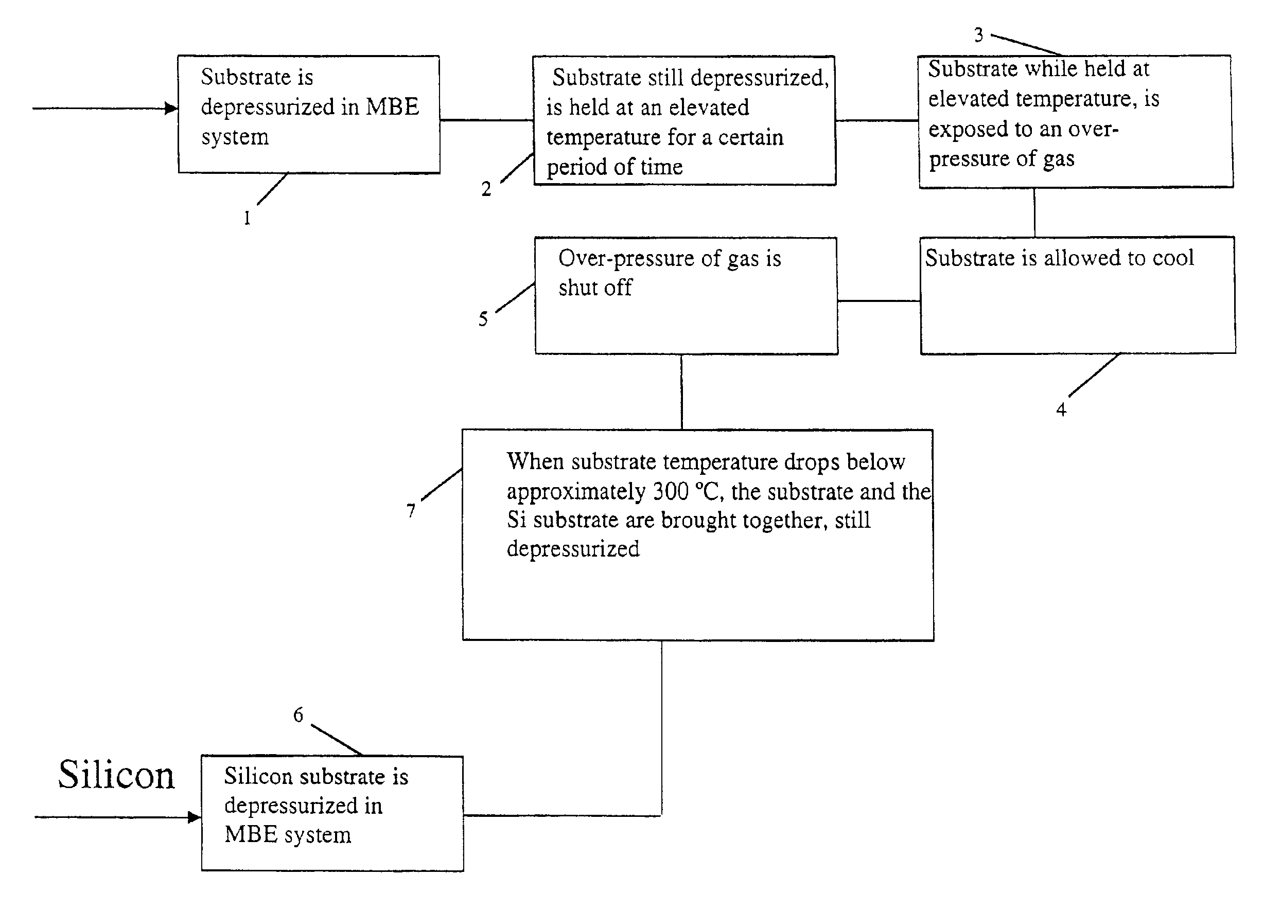
- A method involving a Molecular Beam Epitaxy (MBE) system to create an essentially oxide-free substrate surface by evaporating oxide at elevated temperatures and replacing evaporated atoms with chemisorbed gas atoms, ensuring the crystal structure remains intact and selecting the surface atoms for optimal bonding.

Process Integration and Manufacturing Scalability
The integration of lithographic approaches into substrate bonding processes presents significant challenges and opportunities for manufacturing scalability. Current semiconductor fabrication facilities must adapt existing lithographic infrastructure to accommodate advanced bonding techniques, requiring careful consideration of process flow modifications and equipment compatibility. The transition from traditional thermal bonding methods to lithographically-enhanced approaches necessitates substantial investment in specialized toolsets and process development.
Manufacturing scalability becomes particularly critical when implementing lithographic patterning for surface preparation and alignment features. High-volume production demands require optimization of exposure times, resist processing, and pattern transfer steps to maintain throughput targets. The precision requirements for substrate alignment, often in the sub-micron range, must be balanced against cycle time constraints to ensure economic viability in mass production environments.
Process integration challenges emerge from the need to coordinate multiple lithographic steps with bonding operations while maintaining contamination control and yield targets. Clean room protocols must be enhanced to prevent particle contamination during the extended process sequences, as lithographic steps introduce additional handling and processing stages. Temperature cycling between lithographic processing and bonding operations requires careful thermal budget management to prevent substrate warpage and alignment drift.
Equipment utilization efficiency becomes a key factor in determining the economic feasibility of lithographically-enhanced bonding processes. The sequential nature of lithographic patterning followed by bonding operations can create bottlenecks in production flow, particularly when specialized bonding equipment has limited availability. Parallel processing strategies and optimized scheduling algorithms are essential for maximizing fab utilization rates.
Quality control and metrology requirements expand significantly with the introduction of lithographic steps, necessitating additional inspection points and measurement capabilities. In-line monitoring of pattern fidelity, overlay accuracy, and bonding interface quality requires integration of advanced metrology tools throughout the process flow, impacting both capital investment and operational complexity in high-volume manufacturing environments.
Quality Control and Metrology for Bonded Substrates
Quality control and metrology represent critical aspects of substrate bonding processes, particularly when lithographic approaches are employed to enhance bonding performance. The precision required in advanced semiconductor manufacturing and MEMS applications demands sophisticated measurement techniques capable of detecting nanometer-scale variations in bonding quality. Traditional inspection methods often prove inadequate for evaluating the complex interface characteristics that emerge from lithographically-enhanced bonding processes.
Non-destructive evaluation techniques form the backbone of modern bonding quality assessment. Acoustic microscopy enables detection of voids, delamination, and interface defects through high-frequency ultrasonic waves that penetrate bonded structures. This technique proves particularly valuable for identifying subsurface anomalies that remain invisible to optical inspection methods. Infrared thermography provides complementary information by revealing thermal conductivity variations across bonded interfaces, indicating regions of poor adhesion or incomplete bonding.
Advanced optical metrology systems have evolved to address the unique challenges posed by lithographically-patterned bonding surfaces. Interferometric techniques, including white-light interferometry and phase-shifting interferometry, deliver sub-nanometer height resolution for measuring surface topography and bonding uniformity. These methods prove essential for evaluating the effectiveness of lithographic surface modifications and their impact on final bonding quality.
X-ray inspection technologies offer unparalleled insight into internal bonding structures without requiring sample destruction. High-resolution X-ray computed tomography reveals three-dimensional void distributions and interface morphology, while X-ray photoelectron spectroscopy provides chemical composition analysis of bonding interfaces. These techniques become particularly valuable when assessing the performance of novel lithographic bonding enhancement strategies.
Mechanical testing protocols specifically designed for bonded substrates include die shear testing, pull testing, and four-point bending evaluations. These standardized approaches quantify bond strength and reliability under various stress conditions. Statistical process control methodologies integrate measurement data from multiple metrology techniques to establish comprehensive quality metrics and identify process variations before they impact production yields.
Real-time monitoring systems increasingly incorporate machine learning algorithms to predict bonding quality based on process parameters and in-situ measurements. These predictive quality control approaches enable proactive process adjustments and reduce the reliance on post-bonding inspection, ultimately improving manufacturing efficiency while maintaining stringent quality standards for lithographically-enhanced substrate bonding applications.
Unlock deeper insights with PatSnap Eureka Quick Research — get a full tech report to explore trends and direct your research. Try now!
Generate Your Research Report Instantly with AI Agent
Supercharge your innovation with PatSnap Eureka AI Agent Platform!