Process Control Using Real-Time Computational Lithography Data
APR 24, 20269 MIN READ
Generate Your Research Report Instantly with AI Agent
PatSnap Eureka helps you evaluate technical feasibility & market potential.
Real-Time Lithography Process Control Background and Objectives
Semiconductor lithography has evolved from a relatively straightforward pattern transfer process to one of the most complex manufacturing technologies in modern industry. The continuous push toward smaller feature sizes, following Moore's Law, has driven the development of increasingly sophisticated lithographic systems. Traditional lithography process control relied heavily on post-exposure metrology and feedback mechanisms, which introduced significant delays between pattern exposure and corrective actions. This approach became increasingly inadequate as feature dimensions approached the fundamental limits of optical resolution.
The emergence of computational lithography marked a paradigm shift in how the industry approaches pattern fidelity and process optimization. Techniques such as optical proximity correction, source mask optimization, and inverse lithography have become essential tools for achieving acceptable pattern quality at advanced technology nodes. However, these computational methods have traditionally operated in a predictive mode, calculating corrections based on nominal process conditions rather than real-time manufacturing variations.
Real-time computational lithography represents the convergence of advanced modeling capabilities with high-speed data processing and sensor technologies. This approach enables dynamic adjustment of lithographic parameters during the exposure process itself, rather than relying solely on pre-calculated corrections. The integration of real-time feedback mechanisms addresses the inherent variability in manufacturing processes, including fluctuations in resist properties, substrate topography, and environmental conditions.
The primary objective of implementing real-time computational lithography data for process control is to achieve unprecedented levels of pattern fidelity and manufacturing consistency. This involves developing algorithms capable of processing complex optical and process models within the time constraints of production lithography systems. The target is to reduce critical dimension variation, minimize overlay errors, and improve overall yield through dynamic process optimization.
Another key objective focuses on enabling adaptive manufacturing strategies that can respond to process drift and equipment variations in real-time. This capability is particularly crucial for advanced nodes where traditional process windows have become extremely narrow. The system must demonstrate the ability to maintain pattern quality across varying process conditions while maximizing throughput and minimizing the need for rework.
The ultimate goal extends beyond immediate process improvements to establish a foundation for next-generation lithographic manufacturing. This includes developing the computational infrastructure and algorithmic frameworks necessary to support future technology nodes where static process corrections will be insufficient to meet required specifications.
Market Demand for Advanced Lithography Process Control
The semiconductor industry faces unprecedented challenges in maintaining Moore's Law progression, driving substantial market demand for advanced lithography process control solutions. As feature sizes shrink below 5nm nodes, traditional process control methods prove insufficient for managing the complexity of extreme ultraviolet (EUV) lithography and multi-patterning techniques. This technological gap creates significant market opportunities for real-time computational lithography solutions that can address critical manufacturing challenges.
Market demand stems primarily from leading-edge semiconductor manufacturers who require enhanced yield optimization and defect reduction capabilities. These companies face mounting pressure to achieve higher transistor densities while maintaining cost-effectiveness and production throughput. The increasing complexity of optical proximity correction (OPC) and source mask optimization (SMO) processes necessitates real-time computational solutions that can adapt to manufacturing variations and environmental fluctuations during production.
The automotive semiconductor sector represents another significant demand driver, particularly with the proliferation of advanced driver assistance systems (ADAS) and autonomous vehicle technologies. These applications require extremely high reliability standards, creating demand for sophisticated process control systems that can ensure consistent quality across high-volume production runs. The automotive industry's shift toward electrification further amplifies this demand as power management semiconductors require precise dimensional control.
Data center and artificial intelligence chip manufacturers constitute a rapidly growing market segment demanding advanced lithography process control. The computational requirements for AI workloads drive demand for specialized processors with complex architectures that push lithography capabilities to their limits. These manufacturers require real-time process control systems capable of managing the intricate patterns and tight tolerances necessary for high-performance computing applications.
Mobile device manufacturers continue to drive demand for advanced process control as they pursue thinner form factors and enhanced functionality. The integration of multiple sensors, cameras, and communication modules within compact devices requires sophisticated semiconductor packaging and interconnect technologies that depend on precise lithography control.
The market demand extends beyond traditional semiconductor applications to emerging sectors including quantum computing, photonics, and advanced sensor technologies. These applications often require specialized lithography processes with unique control requirements, creating niche but high-value market opportunities for computational lithography solutions.
Regional demand patterns reflect the global distribution of semiconductor manufacturing, with particularly strong requirements in Asia-Pacific regions where major foundries operate high-volume production facilities. The ongoing geopolitical emphasis on semiconductor supply chain security further intensifies demand for advanced process control technologies across multiple geographic markets.
Current State and Challenges of Real-Time Computational Lithography
Real-time computational lithography represents a paradigm shift from traditional static correction approaches to dynamic, adaptive process control systems. Current implementations primarily focus on offline computational corrections applied during mask design and manufacturing phases, with limited real-time feedback mechanisms during actual wafer exposure processes. The technology landscape shows fragmented development across different lithography equipment manufacturers, each pursuing proprietary solutions for integrating computational models with hardware control systems.
The semiconductor industry has achieved significant progress in developing sophisticated optical proximity correction algorithms and source mask optimization techniques. However, these solutions predominantly operate in pre-processing modes, calculating corrections based on predicted process variations rather than actual real-time measurements. Advanced lithography systems now incorporate limited real-time monitoring capabilities through aerial image sensors and focus monitoring systems, but the integration of comprehensive computational models remains constrained by processing speed limitations.
Major technical challenges persist in achieving true real-time computational lithography implementation. Processing latency represents the most critical bottleneck, as current computational models require substantial processing time that exceeds the millisecond-level response requirements for real-time process control. The complexity of three-dimensional resist modeling, coupled with stochastic effects at advanced technology nodes, demands enormous computational resources that current hardware architectures struggle to deliver within acceptable timeframes.
Data acquisition and sensor integration present additional complexity layers. Existing lithography systems lack comprehensive real-time metrology capabilities necessary to feed accurate process state information into computational models. The challenge extends beyond hardware limitations to include data fusion algorithms capable of synthesizing multiple sensor inputs into actionable correction parameters. Current sensor technologies provide limited spatial resolution and measurement speed, creating gaps between theoretical computational capabilities and practical implementation requirements.
Process variation modeling accuracy remains a fundamental constraint affecting real-time computational lithography effectiveness. While offline models demonstrate reasonable accuracy for nominal process conditions, their predictive capabilities degrade significantly under dynamic process variations encountered during actual production environments. Temperature fluctuations, resist chemistry variations, and mechanical vibrations introduce real-time uncertainties that current computational models inadequately address.
The geographical distribution of technological capabilities shows concentration in advanced semiconductor manufacturing regions, particularly Taiwan, South Korea, and select facilities in the United States and Europe. Research institutions in these regions collaborate closely with equipment manufacturers to develop next-generation computational lithography solutions, though commercial implementations remain limited to specific high-volume manufacturing scenarios where the economic benefits justify the substantial infrastructure investments required.
Existing Real-Time Process Control Solutions
01 Real-time optical proximity correction (OPC) and model-based process control
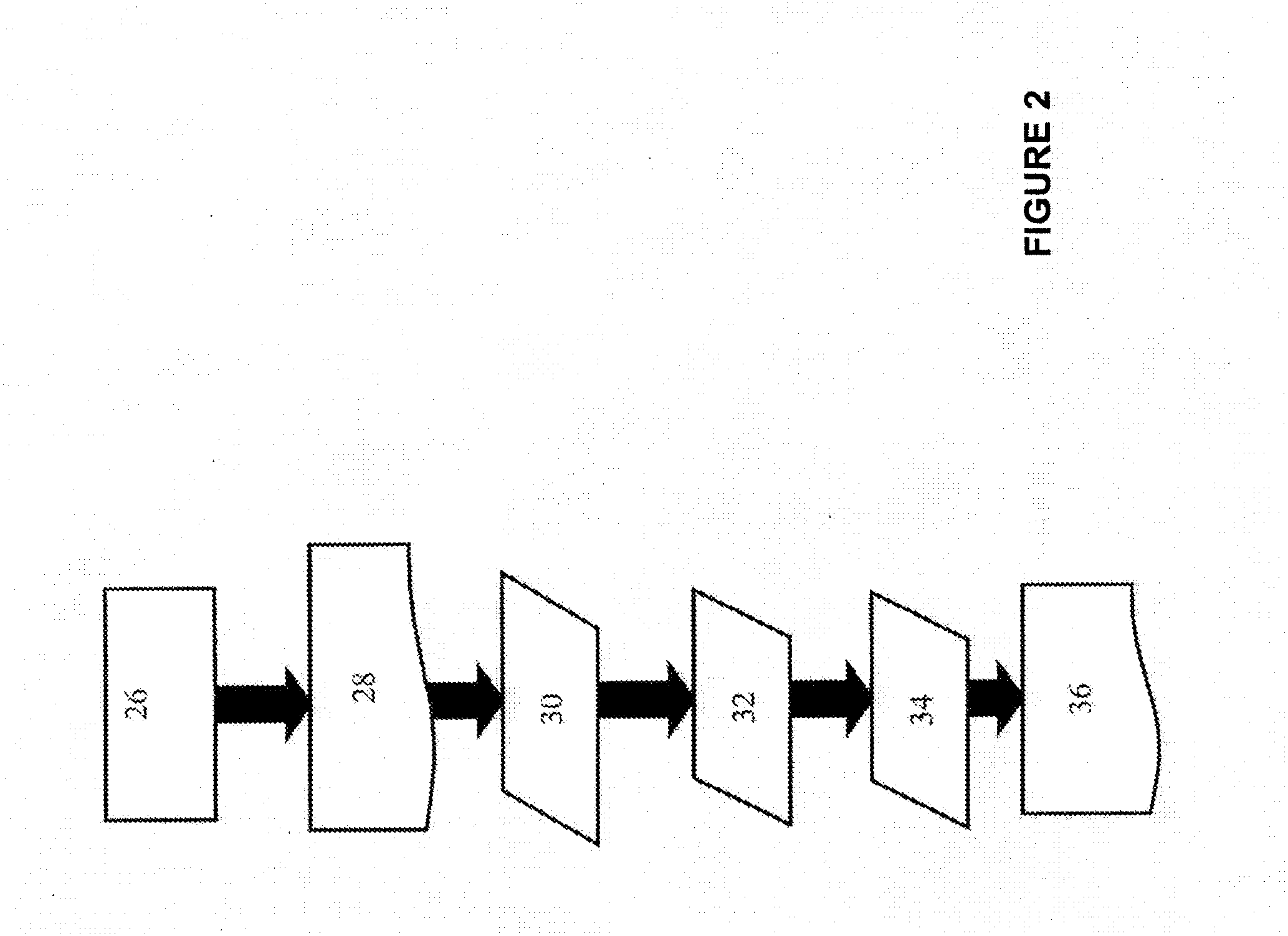
Advanced computational lithography systems employ real-time optical proximity correction techniques to compensate for diffraction and process effects during mask pattern transfer. These systems utilize model-based approaches to predict and correct pattern distortions, enabling dynamic adjustment of lithography parameters. The process control mechanisms incorporate feedback loops that continuously monitor and optimize the lithography process to maintain pattern fidelity and critical dimension uniformity across the wafer.- Real-time optical proximity correction (OPC) and computational lithography optimization: Methods and systems for performing real-time computational lithography involve optimizing mask patterns through optical proximity correction algorithms. These techniques enable dynamic adjustment of lithographic patterns during the manufacturing process to compensate for optical effects and improve pattern fidelity. The optimization process includes iterative calculations that modify mask designs based on simulation results and process parameters to achieve desired wafer patterns.
- Process control and monitoring systems for lithography data processing: Advanced process control systems monitor and regulate lithographic data processing in real-time by collecting process variables and adjusting parameters accordingly. These systems implement feedback mechanisms that track critical dimensions, overlay accuracy, and other quality metrics throughout the lithography workflow. The control systems utilize statistical process control methods and machine learning algorithms to maintain process stability and detect anomalies.
- Parallel and distributed computing architectures for lithography calculations: Computational lithography systems employ parallel processing and distributed computing frameworks to handle the massive data volumes and complex calculations required for real-time processing. These architectures partition lithography computations across multiple processors or computing nodes to achieve the necessary throughput. Hardware acceleration techniques and optimized algorithms enable rapid execution of intensive computational tasks such as mask synthesis and process simulation.
- Data management and workflow optimization for lithography processes: Efficient data management systems handle the storage, retrieval, and processing of large-scale lithography datasets in real-time operations. These systems implement optimized data structures and caching mechanisms to minimize latency in accessing design data and process parameters. Workflow management tools coordinate the sequence of computational lithography operations and ensure proper data flow between different processing stages.
- Machine learning and adaptive control for lithography process optimization: Intelligent control systems incorporate machine learning models and adaptive algorithms to optimize lithography processes based on real-time data analysis. These systems learn from historical process data and current measurements to predict optimal process parameters and make autonomous adjustments. The adaptive control mechanisms continuously refine computational models and correction strategies to improve manufacturing outcomes and reduce cycle times.
02 Parallel processing and distributed computing architectures for lithography data
To handle the massive computational demands of real-time lithography data processing, distributed computing architectures are employed. These systems utilize parallel processing techniques to partition lithography data into smaller segments that can be processed simultaneously across multiple computing nodes. The architecture enables efficient load balancing and resource allocation, significantly reducing the overall processing time while maintaining data integrity and computational accuracy.Expand Specific Solutions03 Machine learning and artificial intelligence for process optimization
Modern computational lithography systems integrate machine learning algorithms and artificial intelligence techniques to enhance process control capabilities. These systems learn from historical process data to predict optimal lithography parameters and identify potential defects before they occur. The AI-driven approach enables adaptive process control that can automatically adjust to variations in manufacturing conditions, improving yield and reducing cycle time.Expand Specific Solutions04 Real-time metrology integration and feedback control systems
Integration of real-time metrology systems with computational lithography enables continuous monitoring and feedback control during the manufacturing process. These systems collect measurement data from various sensors and inspection tools, processing the information in real-time to detect deviations from target specifications. The feedback control mechanisms automatically adjust process parameters to maintain optimal performance and minimize defects throughout the production run.Expand Specific Solutions05 Data compression and efficient storage solutions for lithography patterns
Efficient data management is critical for real-time computational lithography, requiring advanced compression algorithms and storage solutions to handle large volumes of mask data. These systems implement hierarchical data structures and intelligent caching mechanisms to enable rapid access to frequently used pattern data. The compression techniques reduce data transfer bandwidth requirements while maintaining lossless pattern information, facilitating faster processing and reduced storage costs.Expand Specific Solutions
Key Players in Lithography Equipment and Software Industry
The process control using real-time computational lithography data represents a rapidly evolving segment within the semiconductor manufacturing industry, currently in its growth phase with significant technological advancement opportunities. The market demonstrates substantial scale potential, driven by increasing demand for precision manufacturing in advanced node production. Technology maturity varies significantly across key players, with established leaders like ASML Netherlands BV and Applied Materials setting industry standards through their advanced lithography and process control solutions. Major foundries including Taiwan Semiconductor Manufacturing Co. and GLOBALFOUNDRIES are actively implementing these technologies, while equipment manufacturers such as Tokyo Electron, KLA Corp, and Nova Ltd. contribute specialized metrology and process control capabilities. Emerging players like Shanghai Microelectronics Equipment and Semiconductor Manufacturing International are developing competitive solutions, indicating a dynamic competitive landscape with both established Western companies and rising Asian manufacturers driving innovation in real-time computational lithography process control systems.
ASML Netherlands BV
Technical Solution: ASML has developed advanced computational lithography solutions integrated with real-time process control for their extreme ultraviolet (EUV) lithography systems. Their approach combines machine learning algorithms with high-speed data processing to analyze lithographic patterns in real-time, enabling immediate corrections during the exposure process. The system utilizes predictive modeling to anticipate potential defects and automatically adjusts exposure parameters, dose control, and overlay corrections. Their computational lithography platform processes terabytes of data per wafer, implementing advanced optical proximity correction (OPC) and source mask optimization (SMO) techniques that adapt dynamically based on real-time feedback from metrology systems integrated within the lithography tool.
Strengths: Market leader in EUV technology with most advanced real-time correction capabilities. Weaknesses: Extremely high cost and complexity limiting accessibility to only leading-edge fabs.
Taiwan Semiconductor Manufacturing Co., Ltd.
Technical Solution: TSMC has implemented comprehensive real-time computational lithography control systems across their advanced node production lines. Their solution integrates machine learning-based process control with advanced pattern recognition algorithms to monitor and adjust lithographic processes in real-time. The system employs predictive analytics to optimize exposure conditions, resist processing parameters, and overlay accuracy based on continuous feedback from inline metrology tools. TSMC's approach includes real-time dose correction, focus optimization, and automated defect classification systems that can make millisecond adjustments during wafer processing. Their computational framework processes real-time data from multiple sensors and metrology points to maintain critical dimension uniformity and pattern fidelity across entire wafers.
Strengths: Extensive manufacturing experience with proven high-volume implementation of real-time control systems. Weaknesses: Solutions are primarily developed for internal use with limited external technology transfer.
Core Technologies in Real-Time Lithography Data Processing
Computational Process Control
PatentActiveUS20120303151A1
Innovation
- The implementation of computational process control (CPC) systems that analyze temporal drift and use wafer metrology data to optimize lithography apparatuses and processes, maintaining performance close to a pre-defined baseline through feedback loops and scanner matching, while compensating for non-scanner effects like resist process drift.
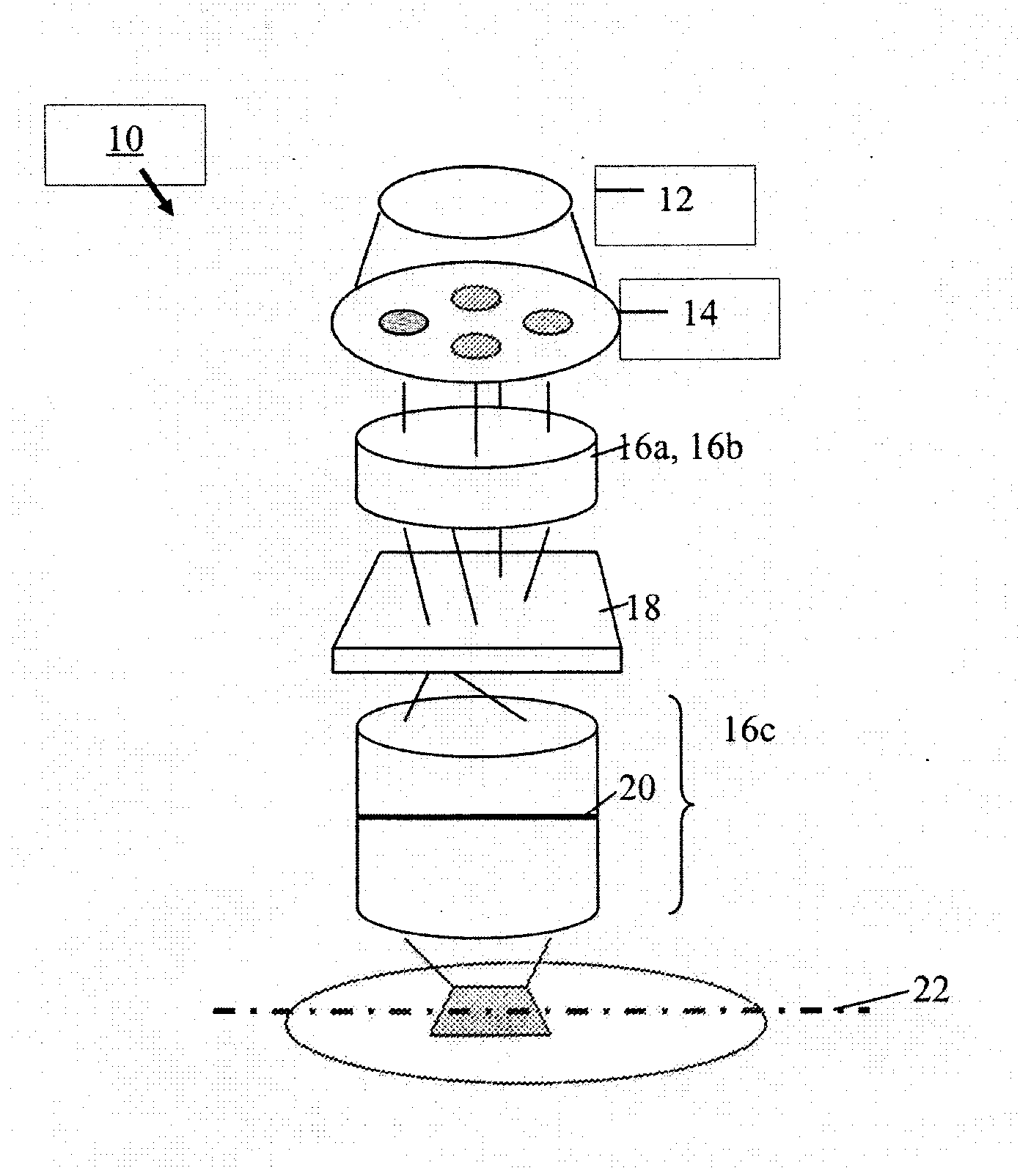
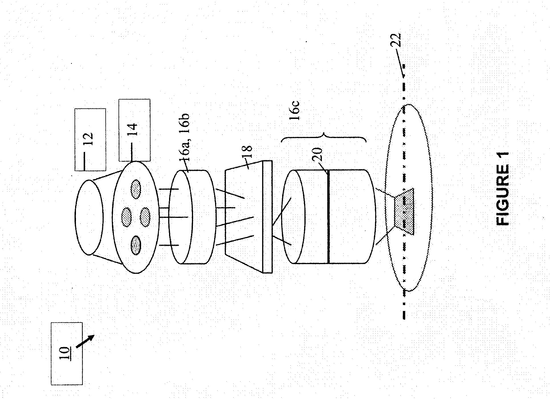

Computational process control
PatentActiveJP2016048399A
Innovation
- Implementing a scanner stability control system that uses wafer metrology data to monitor and adjust lithographic apparatus settings, maintaining performance near predefined baseline conditions through feedback loops and compensation for drift, thereby optimizing process windows and reducing the need for recalibration.


Semiconductor Manufacturing Standards and Compliance
The integration of real-time computational lithography data into semiconductor manufacturing processes necessitates adherence to stringent industry standards and regulatory compliance frameworks. Current semiconductor manufacturing operates under established standards such as SEMI E10 for equipment automation, SEMI E30 for generic model for communications and control, and ISO 26262 for functional safety in automotive semiconductors. These standards provide the foundational framework for implementing advanced process control systems that utilize computational lithography data.
Regulatory compliance in semiconductor manufacturing encompasses multiple dimensions, including environmental regulations like RoHS and REACH, quality management systems under ISO 9001 and AS9100 for aerospace applications, and cybersecurity standards such as IEC 62443 for industrial automation systems. The implementation of real-time computational lithography data processing must align with these existing compliance requirements while maintaining data integrity and traceability throughout the manufacturing workflow.
International standards organizations including SEMI, IEEE, and IEC have established specific guidelines for semiconductor process control systems. SEMI E125 standard addresses advanced process control requirements, while IEEE 1451 series standards define smart transducer interfaces that are crucial for real-time data acquisition from lithography systems. These standards ensure interoperability between different equipment vendors and maintain consistency in data formats and communication protocols.
Quality assurance frameworks such as Six Sigma and Statistical Process Control (SPC) methodologies must be integrated with real-time computational lithography systems to meet industry compliance requirements. The implementation requires validation protocols that demonstrate system reliability, repeatability, and accuracy according to FDA 21 CFR Part 11 for electronic records and signatures, particularly relevant for medical device semiconductor applications.
Emerging compliance challenges include data privacy regulations like GDPR for European operations and export control regulations such as EAR and ITAR that govern the transfer of advanced semiconductor technologies. Real-time computational lithography systems must incorporate appropriate data handling and access control mechanisms to ensure compliance with these evolving regulatory landscapes while maintaining operational efficiency and technological advancement capabilities.
Integration Challenges with Existing Fab Infrastructure
The integration of real-time computational lithography data into existing semiconductor fabrication infrastructure presents multifaceted challenges that require careful consideration of legacy systems, data flow architectures, and operational continuity. Modern fabs operate with established process control frameworks that were designed around traditional metrology and feedback mechanisms, creating inherent compatibility issues when introducing advanced computational lithography solutions.
Legacy equipment compatibility represents a primary obstacle, as existing lithography tools, metrology systems, and process control software often lack the necessary interfaces and computational capabilities to handle real-time CL data streams. Many fabs operate with equipment spanning multiple technology generations, where older systems may require significant hardware upgrades or complete replacement to support the high-bandwidth data requirements and processing demands of real-time computational lithography.
Data infrastructure limitations pose another critical challenge, particularly regarding network bandwidth, storage capacity, and processing power requirements. Real-time CL generates massive data volumes that must be transmitted, processed, and stored without disrupting existing fab operations. The current IT infrastructure in many facilities was not designed to handle such intensive computational workloads, necessitating substantial investments in high-performance computing resources and network upgrades.
Software integration complexity emerges from the need to seamlessly connect new CL algorithms with existing manufacturing execution systems, statistical process control platforms, and equipment automation software. This integration requires extensive customization and validation to ensure data consistency, maintain process traceability, and preserve existing quality control protocols while introducing new computational capabilities.
Operational workflow disruption presents significant concerns, as implementing real-time CL systems often requires modifications to established production procedures, operator training programs, and maintenance schedules. The transition period can impact fab productivity and yield performance, requiring careful change management strategies to minimize operational risks while maximizing the benefits of advanced process control capabilities.
Unlock deeper insights with PatSnap Eureka Quick Research — get a full tech report to explore trends and direct your research. Try now!
Generate Your Research Report Instantly with AI Agent
Supercharge your innovation with PatSnap Eureka AI Agent Platform!