Parameter-Driven Lithography Strategies for Accurate Patterning
APR 24, 202610 MIN READ
Generate Your Research Report Instantly with AI Agent
PatSnap Eureka helps you evaluate technical feasibility & market potential.
Parameter-Driven Lithography Background and Objectives
Parameter-driven lithography represents a paradigm shift in semiconductor manufacturing, emerging from the increasing complexity of modern integrated circuit fabrication. As device dimensions continue to shrink below 10 nanometers, traditional lithographic approaches face fundamental physical limitations that threaten the continuation of Moore's Law. The evolution from simple contact printing to advanced extreme ultraviolet (EUV) lithography has been marked by continuous refinement of process parameters to achieve unprecedented pattern fidelity.
The historical development of lithography has consistently demonstrated that parameter optimization is crucial for overcoming resolution barriers. Early photolithography systems relied on basic exposure dose and focus adjustments, but contemporary systems require sophisticated control of dozens of interdependent variables including illumination conditions, mask bias, optical proximity corrections, and resist chemistry parameters. This complexity has driven the need for systematic, data-driven approaches to parameter selection and optimization.
Current market demands for higher transistor density, improved performance, and reduced power consumption have intensified the pressure on lithographic processes. The semiconductor industry's transition to advanced nodes such as 5nm and 3nm technologies requires pattern accuracy tolerances measured in fractions of nanometers, making parameter-driven strategies essential rather than optional. Manufacturing yield and cost considerations further emphasize the importance of robust parameter control methodologies.
The primary objective of parameter-driven lithography strategies is to establish systematic frameworks for optimizing multiple process variables simultaneously to achieve target pattern specifications. This involves developing predictive models that can accurately forecast lithographic outcomes based on parameter inputs, enabling proactive process control rather than reactive adjustments. The approach aims to minimize critical dimension variation, reduce line edge roughness, and eliminate pattern defects through intelligent parameter selection.
Advanced computational lithography techniques now enable real-time parameter optimization using machine learning algorithms and physics-based modeling. These methods seek to identify optimal parameter combinations that maximize process windows while maintaining manufacturing throughput requirements. The integration of metrology feedback with parameter adjustment algorithms represents a key technological goal for achieving closed-loop process control.
The ultimate vision for parameter-driven lithography encompasses fully autonomous manufacturing systems capable of self-optimization based on product requirements and process constraints. This transformative approach promises to extend the viability of optical lithography techniques while providing the foundation for next-generation patterning technologies including directed self-assembly and nanoimprint lithography applications.
Market Demand for Advanced Lithography Solutions
The semiconductor industry faces unprecedented challenges in achieving precise patterning at advanced technology nodes, driving substantial market demand for sophisticated lithography solutions. As device geometries continue to shrink below 7nm and approach 3nm processes, traditional lithography approaches encounter fundamental physical limitations that necessitate parameter-driven strategies for maintaining manufacturing yield and device performance.
Market demand stems primarily from leading semiconductor manufacturers who require enhanced process control capabilities to address critical dimension uniformity, overlay accuracy, and defect density challenges. These manufacturers are actively seeking lithography solutions that can dynamically adjust exposure parameters based on real-time feedback and predictive modeling to compensate for systematic and random variations across wafer surfaces.
The automotive semiconductor sector represents a rapidly expanding market segment demanding high-reliability lithography solutions. Advanced driver assistance systems and electric vehicle power management chips require precise patterning with stringent quality standards, creating opportunities for parameter-driven lithography technologies that can ensure consistent performance across diverse operating conditions.
Memory manufacturers constitute another significant demand driver, particularly for 3D NAND and advanced DRAM production. These applications require exceptional aspect ratio control and sidewall profile accuracy, which parameter-driven approaches can address through adaptive exposure strategies and real-time process optimization algorithms.
Emerging applications in artificial intelligence accelerators, quantum computing components, and photonic integrated circuits are generating new market requirements for specialized lithography capabilities. These applications often involve novel materials and unconventional device architectures that benefit from flexible, parameter-adjustable lithography processes capable of handling diverse patterning challenges within single manufacturing workflows.
The market demand is further amplified by increasing cost pressures in semiconductor manufacturing, where parameter-driven lithography strategies offer potential solutions for improving yield rates and reducing rework cycles. Manufacturers are particularly interested in solutions that can minimize the need for multiple mask layers while maintaining pattern fidelity through intelligent parameter optimization.
Regional market dynamics show strong demand concentration in Asia-Pacific manufacturing hubs, with significant growth potential in European and North American advanced research facilities focusing on next-generation semiconductor technologies and specialized applications requiring precise patterning control.
Current Lithography Parameter Control Challenges
Modern lithography systems face unprecedented challenges in parameter control as semiconductor manufacturing pushes toward increasingly smaller feature sizes and higher pattern densities. The complexity of managing multiple interdependent parameters simultaneously has become a critical bottleneck in achieving consistent, high-yield production. Traditional control methodologies struggle to maintain the precision required for advanced nodes, where even minor parameter deviations can result in significant pattern distortions or complete process failures.
Exposure dose control represents one of the most fundamental challenges in contemporary lithography operations. The relationship between dose uniformity and pattern fidelity becomes increasingly sensitive as feature dimensions shrink below 10 nanometers. Current systems often exhibit dose variations across the wafer surface due to illumination non-uniformities, resist sensitivity fluctuations, and thermal effects during exposure. These variations directly translate to critical dimension variations that can exceed acceptable tolerances for advanced semiconductor devices.
Focus control presents another layer of complexity, particularly in high numerical aperture systems where depth of field margins are extremely narrow. Wafer topography variations, thermal expansion during processing, and mechanical vibrations contribute to focus errors that compromise pattern quality. The challenge is compounded by the need to maintain focus accuracy across entire wafer surfaces while accounting for process-induced wafer distortions and chuck-related height variations.
Overlay accuracy has emerged as perhaps the most stringent parameter control challenge in multi-layer device fabrication. Sub-nanometer overlay requirements demand unprecedented precision in stage positioning, wafer alignment, and distortion correction. Current systems struggle with dynamic overlay errors caused by wafer processing history, thermal cycling effects, and time-dependent mechanical drift. The interaction between overlay errors and other lithographic parameters creates complex feedback loops that are difficult to predict and control.
Temperature and environmental stability present additional control challenges that significantly impact lithographic performance. Resist temperature variations affect chemical reaction kinetics and material properties, leading to process variations that manifest as pattern irregularities. Ambient temperature fluctuations cause mechanical component expansion and contraction, affecting optical alignment and stage positioning accuracy. Humidity control becomes critical for resist processing and electrostatic discharge prevention, yet maintaining stable environmental conditions across large manufacturing facilities remains technically challenging.
The integration of multiple parameter control systems creates systematic challenges related to parameter coupling and cross-talk effects. Adjustments made to correct one parameter often inadvertently affect others, creating optimization conflicts that require sophisticated control algorithms. Real-time parameter monitoring and feedback systems generate vast amounts of data that must be processed and acted upon within tight temporal constraints, pushing current computational capabilities to their limits.
Existing Parameter Optimization Solutions
01 Model-based optical proximity correction (OPC) for lithography accuracy
Advanced lithography strategies employ model-based optical proximity correction techniques to compensate for optical diffraction effects and process variations. These methods use computational models to predict and correct pattern distortions before mask fabrication, adjusting feature geometries based on parameters such as feature size, pitch, and local pattern density. The correction algorithms optimize mask patterns to achieve target dimensions on wafer, significantly improving pattern fidelity and critical dimension control across various process windows.- Model-based optical proximity correction (OPC) for pattern fidelity: Advanced lithography strategies employ model-based optical proximity correction techniques that use computational models to predict and compensate for optical distortions during pattern transfer. These methods analyze design layouts and apply systematic corrections to mask patterns based on process parameters such as wavelength, numerical aperture, and resist characteristics. The approach enables accurate reproduction of intended geometries by pre-distorting mask features to counteract known lithographic effects, thereby improving critical dimension control and pattern fidelity across various feature sizes and densities.
- Parameter optimization through machine learning and computational lithography: Lithography accuracy can be enhanced through intelligent parameter optimization using machine learning algorithms and computational methods. These techniques analyze relationships between process variables including exposure dose, focus settings, and mask bias to identify optimal parameter combinations. By training models on empirical data or simulation results, the systems can predict lithographic outcomes and automatically adjust parameters to minimize pattern errors. This data-driven approach enables adaptive process control that responds to variations in manufacturing conditions and improves yield.
- Source-mask optimization (SMO) for resolution enhancement: Source-mask optimization represents a co-optimization strategy where both illumination source characteristics and mask patterns are simultaneously adjusted to achieve superior patterning results. This technique manipulates parameters such as illumination pupil shape, polarization, and mask transmission properties to maximize process windows and extend lithographic capabilities beyond conventional limits. The methodology employs iterative optimization algorithms that balance competing objectives including depth of focus, exposure latitude, and pattern contrast to deliver robust patterning solutions for complex geometries.
- Multi-patterning decomposition and overlay control: For features below single-exposure resolution limits, multi-patterning strategies decompose complex layouts into multiple simpler mask layers that are sequentially exposed and processed. Parameter-driven approaches optimize the decomposition algorithms and overlay alignment between successive patterning steps to minimize stitching errors and maintain dimensional accuracy. These methods incorporate process variation models and employ sophisticated metrology feedback to adjust exposure parameters for each patterning layer, ensuring that the combined result matches design intent despite the increased process complexity.
- Dose and focus control with advanced metrology feedback: Precise control of exposure dose and focus parameters is critical for accurate pattern reproduction, particularly for advanced technology nodes. Modern lithography systems integrate real-time metrology and feedback mechanisms that continuously monitor pattern quality metrics and adjust exposure parameters accordingly. These closed-loop control systems utilize measurements of critical dimensions, sidewall angles, and pattern placement to dynamically optimize dose and focus settings across the wafer, compensating for systematic variations and random fluctuations to maintain tight process control and improve manufacturing consistency.
02 Source-mask optimization (SMO) techniques
Parameter-driven lithography employs simultaneous optimization of illumination source and mask patterns to maximize imaging performance. This approach adjusts source shapes, polarization states, and mask transmission characteristics based on target pattern requirements and process constraints. The optimization process considers multiple parameters including depth of focus, exposure latitude, and pattern fidelity to determine optimal configurations that enhance resolution and process robustness for complex patterns.Expand Specific Solutions03 Computational lithography with machine learning integration
Modern lithography strategies incorporate machine learning algorithms to optimize patterning parameters and predict lithographic outcomes. These systems analyze historical process data and simulation results to establish relationships between input parameters and pattern quality metrics. The learned models enable rapid parameter optimization, defect prediction, and process window determination, reducing the need for extensive physical testing while improving accuracy in pattern transfer.Expand Specific Solutions04 Multi-patterning decomposition and coloring strategies
Advanced patterning approaches utilize decomposition algorithms to split complex patterns into multiple simpler exposures that can be manufactured within lithographic constraints. These strategies employ graph-based coloring algorithms and optimization techniques to assign features to different mask layers while minimizing conflicts and maintaining pattern integrity. The decomposition process considers parameters such as minimum pitch, overlay tolerance, and stitching requirements to ensure accurate final pattern formation through sequential exposures.Expand Specific Solutions05 Dose and focus optimization for process window enhancement
Lithography accuracy is enhanced through systematic optimization of exposure dose and focus parameters across the wafer field. These strategies employ metrology feedback and computational models to determine optimal parameter settings that maximize common process windows for all critical features. The optimization considers local pattern characteristics, substrate topography, and lens aberrations to establish spatially-varying parameter maps that compensate for systematic variations and improve overall patterning uniformity.Expand Specific Solutions
Key Players in Advanced Lithography Equipment Industry
The parameter-driven lithography landscape represents a mature yet rapidly evolving sector within the semiconductor manufacturing industry, currently valued at approximately $15-20 billion globally. The industry is in an advanced consolidation phase, dominated by established equipment manufacturers and leading foundries. Technology maturity varies significantly across different lithography approaches, with ASML Netherlands BV maintaining leadership in EUV systems, while traditional players like Nikon Corp. and Canon Inc. focus on DUV technologies. Major foundries including Taiwan Semiconductor Manufacturing Co. and Samsung Electronics Co. drive innovation through advanced process requirements. Equipment suppliers such as Applied Materials Inc. and Lam Research Corp. provide complementary processing solutions, while emerging players like ChangXin Memory Technologies represent growing regional capabilities. The competitive landscape reflects high barriers to entry, substantial R&D investments, and increasing specialization in parameter optimization for next-generation node requirements.
ASML Netherlands BV
Technical Solution: ASML leads parameter-driven lithography with advanced Extreme Ultraviolet (EUV) lithography systems that utilize sophisticated computational lithography algorithms. Their technology employs machine learning-based optical proximity correction (OPC) and source mask optimization (SMO) techniques to achieve sub-7nm patterning accuracy. The company's Twinscan NXE series integrates real-time parameter adjustment capabilities, enabling dynamic correction of overlay errors within 1nm precision. Their holistic lithography approach combines advanced metrology, computational modeling, and closed-loop control systems to optimize critical dimension uniformity and pattern fidelity across entire wafers.
Strengths: Market leadership in EUV technology with unmatched resolution capabilities and comprehensive computational lithography solutions. Weaknesses: Extremely high equipment costs and complex maintenance requirements limiting accessibility.
Taiwan Semiconductor Manufacturing Co., Ltd.
Technical Solution: TSMC implements comprehensive parameter-driven lithography strategies across their advanced node manufacturing processes, particularly for 3nm and 5nm technologies. Their approach integrates advanced process control (APC) systems with real-time lithography parameter optimization, including dose and focus control within tight tolerances. TSMC utilizes machine learning algorithms to predict and compensate for systematic variations in lithography processes, achieving critical dimension control within ±2nm across 300mm wafers. Their methodology combines multi-patterning techniques with computational lithography to enable accurate pattern transfer for complex semiconductor designs with billions of transistors.
Strengths: World-class manufacturing expertise with proven high-volume production capabilities and advanced process control systems. Weaknesses: Heavy dependence on external lithography equipment suppliers and high capital investment requirements.
Core Innovations in Lithography Parameter Control
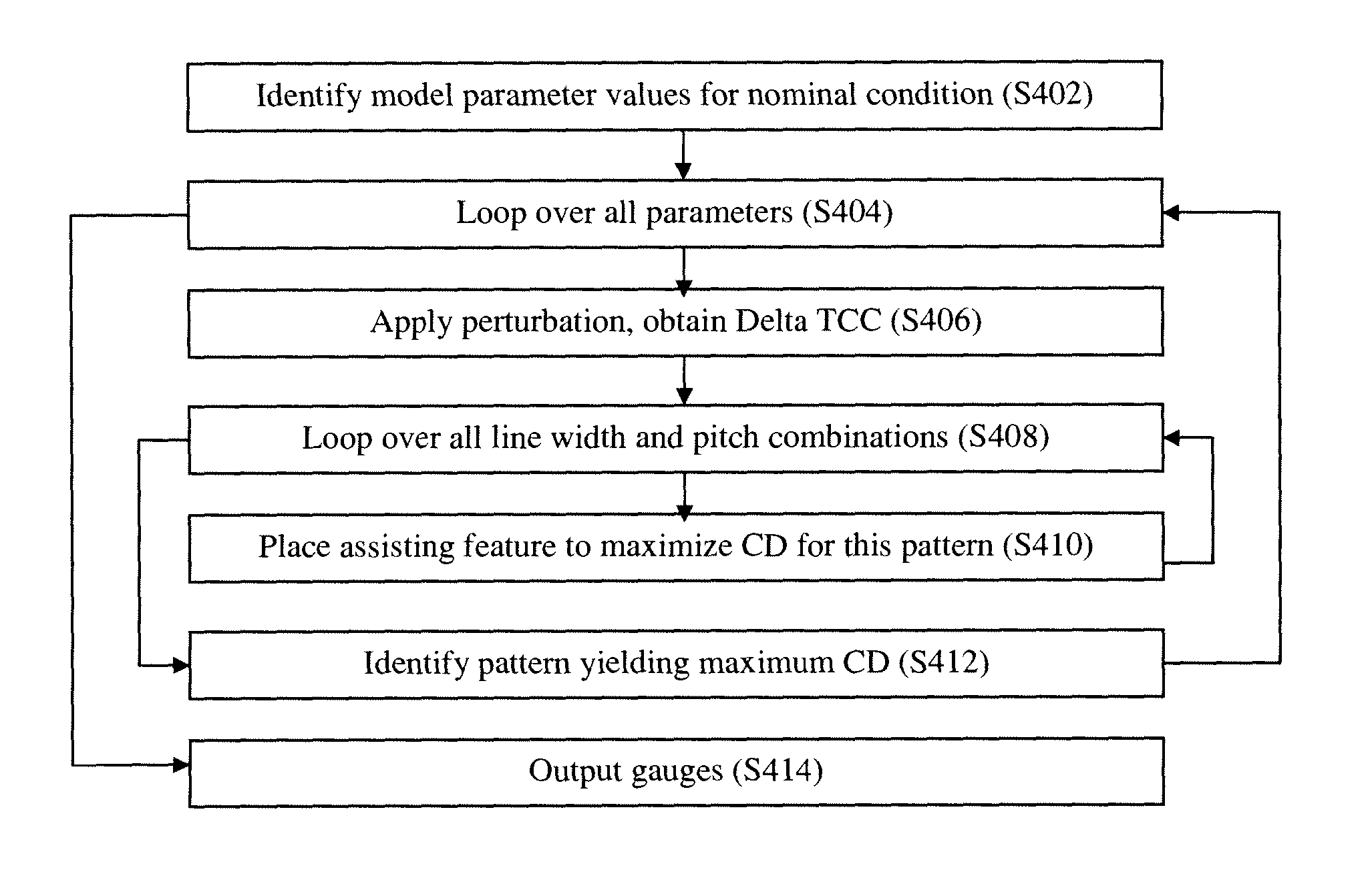
Methods and Systems for Parameter-Sensitive and Orthogonal Gauge Design for Lithography Calibration
PatentInactiveUS20110224956A1
Innovation
- The development of computationally efficient techniques for designing gauge patterns that are extremely sensitive to parameter variations, involving the identification of optimal line width/pitch combinations and assist feature placement to maximize CD changes, and transforming the model parametric space to enhance sensitivity and robustness against measurement errors.

A method for optimizing a parameter applied in a semiconductor fabrication process including a lithography step
PatentInactiveEP4372468A1
Innovation
- A method involving the use of a metrology target pattern with asymmetric marks, each with different design critical dimensions, is printed multiple times with varying focus settings, allowing for the determination of optimized parameter settings by assessing the slope of the effective critical dimension versus design critical dimension relation, which is more sensitive and independent of dose settings.


Semiconductor Manufacturing Standards and Regulations
The semiconductor manufacturing industry operates under a comprehensive framework of standards and regulations that directly impact parameter-driven lithography strategies for accurate patterning. International standards organizations such as SEMI, IEEE, and ISO have established critical guidelines that govern lithography processes, equipment specifications, and quality control measures. These standards ensure consistency across global manufacturing facilities and provide benchmarks for process optimization and yield improvement.
SEMI standards play a particularly crucial role in defining equipment interfaces, safety protocols, and process control requirements for lithography systems. Standards like SEMI E10 for equipment automation and SEMI E30 for generic model specifications directly influence how parameter-driven lithography strategies are implemented and monitored. These regulations mandate specific data collection protocols, process variable tracking, and statistical process control methods that are essential for maintaining patterning accuracy.
Environmental and safety regulations significantly impact lithography operations, particularly regarding chemical handling, waste disposal, and worker exposure limits. The implementation of parameter-driven strategies must comply with OSHA regulations, EPA guidelines, and local environmental standards. These requirements often necessitate specific process modifications, containment systems, and monitoring protocols that can affect lithography parameter optimization and process windows.
Quality management standards such as ISO 9001 and automotive-specific standards like IATF 16949 establish rigorous documentation and traceability requirements for lithography processes. These standards mandate comprehensive parameter tracking, statistical analysis, and continuous improvement methodologies that directly support parameter-driven lithography strategies. The required quality systems ensure that process variations are systematically identified, analyzed, and corrected to maintain patterning accuracy.
Export control regulations and technology transfer restrictions also influence the development and implementation of advanced lithography strategies. ITAR regulations, EAR controls, and international trade agreements can limit access to certain technologies, materials, or process knowledge, potentially constraining the optimization of parameter-driven approaches. Compliance with these regulations requires careful consideration of technology sharing, equipment sourcing, and process development activities.
Regional regulatory differences create additional complexity for global semiconductor manufacturers implementing standardized parameter-driven lithography strategies. Variations in environmental standards, safety requirements, and quality certifications across different countries necessitate flexible process control systems that can adapt to local regulatory requirements while maintaining consistent patterning performance and accuracy standards.
Process Integration Challenges in Advanced Node Manufacturing
The integration of parameter-driven lithography strategies into advanced node manufacturing presents multifaceted challenges that extend beyond individual process optimization. As semiconductor devices scale to sub-5nm nodes, the interdependencies between lithography parameters and subsequent manufacturing steps create complex integration bottlenecks that require systematic resolution approaches.
Thermal budget management emerges as a critical constraint when implementing parameter-driven lithography strategies. The optimized exposure and development parameters often necessitate specific temperature profiles that may conflict with downstream processes such as ion implantation, metallization, and chemical mechanical planarization. The cumulative thermal exposure across multiple patterning steps can lead to pattern distortion, resist flow, and dimensional instability, particularly in multi-patterning schemes where precise overlay control is paramount.
Material compatibility issues compound integration complexity as parameter-driven approaches frequently require specialized resist formulations, anti-reflective coatings, and etch chemistries. These materials must maintain compatibility with existing process flows while delivering the enhanced performance characteristics demanded by advanced lithography strategies. The introduction of new materials often triggers extensive qualification cycles and may necessitate modifications to cleaning protocols, contamination control measures, and equipment maintenance procedures.
Process window overlap represents another significant integration challenge, where the optimized parameter sets for lithography must align with the operational windows of adjacent processes. The narrow process margins inherent in advanced nodes mean that lithography parameter optimization cannot occur in isolation but must consider the cumulative impact on yield and device performance. This requires sophisticated process modeling and extensive design of experiments to identify viable integration pathways.
Equipment throughput and cycle time considerations further complicate integration efforts. Parameter-driven strategies often involve increased process complexity, additional metrology steps, and enhanced process control requirements that can significantly impact manufacturing throughput. The economic viability of these approaches depends on achieving acceptable cost-per-wafer metrics while maintaining the quality improvements that justify their implementation.
Cross-contamination risks and process isolation requirements add another layer of complexity, particularly when parameter-driven strategies involve novel chemistries or processing conditions that may not be compatible with standard manufacturing environments. This necessitates careful evaluation of equipment sharing strategies and may require dedicated processing tools or enhanced isolation protocols.
Unlock deeper insights with PatSnap Eureka Quick Research — get a full tech report to explore trends and direct your research. Try now!
Generate Your Research Report Instantly with AI Agent
Supercharge your innovation with PatSnap Eureka AI Agent Platform!