Microfluidic Device Fabrication Utilizing Computational Lithography
APR 24, 20269 MIN READ
Generate Your Research Report Instantly with AI Agent
PatSnap Eureka helps you evaluate technical feasibility & market potential.
Microfluidic Computational Lithography Background and Objectives
Microfluidic technology has emerged as a transformative field that manipulates fluids at the microscale, typically involving channels with dimensions ranging from tens to hundreds of micrometers. This technology enables precise control of fluid flow, mixing, and reaction processes within miniaturized devices, making it invaluable for applications in biomedical diagnostics, drug discovery, chemical synthesis, and environmental monitoring. The ability to handle minute volumes of samples and reagents while maintaining high precision has positioned microfluidics as a cornerstone technology for lab-on-a-chip systems and point-of-care diagnostics.
The evolution of microfluidic device fabrication has progressed through several distinct phases, beginning with traditional photolithography techniques adapted from semiconductor manufacturing. Early approaches relied on standard UV lithography with chrome masks, which provided adequate resolution for basic channel geometries but faced limitations in creating complex three-dimensional structures and achieving sub-micrometer features. As applications demanded higher precision and more sophisticated geometries, the field has increasingly turned toward advanced fabrication methodologies.
Computational lithography represents a paradigm shift in microfluidic device manufacturing, leveraging sophisticated algorithms and computational models to optimize the lithographic process. This approach encompasses optical proximity correction, phase-shift masking, and resolution enhancement techniques that were originally developed for semiconductor manufacturing but are now being adapted for microfluidic applications. The integration of computational methods enables the creation of features with improved fidelity, reduced edge roughness, and enhanced dimensional control.
The primary objective of implementing computational lithography in microfluidic device fabrication is to achieve unprecedented precision in channel geometry while enabling the creation of complex three-dimensional structures that were previously unattainable. This includes the ability to fabricate gradient channels, curved pathways, and intricate mixing structures with nanometer-scale accuracy. Additionally, computational lithography aims to improve manufacturing reproducibility and reduce defect rates, which are critical factors for commercial viability.
Current technological goals focus on developing integrated computational frameworks that can predict and compensate for process variations, optimize exposure patterns for specific microfluidic geometries, and enable rapid prototyping of novel device architectures. The ultimate vision encompasses fully automated design-to-fabrication workflows where computational models directly translate functional requirements into optimized lithographic patterns, significantly reducing development time and manufacturing costs while expanding the boundaries of achievable microfluidic device complexity.
Market Demand for Advanced Microfluidic Manufacturing
The global microfluidics market has experienced substantial growth driven by increasing demand for point-of-care diagnostics, personalized medicine, and high-throughput biological analysis. Healthcare applications represent the largest segment, with particular emphasis on rapid diagnostic testing, drug discovery platforms, and single-cell analysis systems. The COVID-19 pandemic significantly accelerated adoption of microfluidic-based diagnostic devices, highlighting the critical need for rapid, accurate, and portable testing solutions.
Pharmaceutical and biotechnology companies are increasingly adopting advanced microfluidic manufacturing technologies to develop sophisticated drug delivery systems and organ-on-chip platforms. These applications require precise control over channel geometries, surface properties, and fluid dynamics, driving demand for more sophisticated fabrication techniques beyond traditional soft lithography methods.
The diagnostics sector shows particularly strong growth potential, with increasing requirements for multiplexed assays, reduced sample volumes, and faster time-to-result. Clinical laboratories and research institutions are seeking microfluidic devices capable of performing complex biochemical analyses with enhanced sensitivity and specificity, necessitating advanced manufacturing approaches that can achieve sub-micron feature resolution and complex three-dimensional architectures.
Environmental monitoring and food safety applications represent emerging market segments where microfluidic devices offer advantages in portability, cost-effectiveness, and real-time analysis capabilities. These applications often require robust devices capable of handling complex sample matrices, driving demand for manufacturing techniques that can produce durable, chemically resistant microfluidic systems.
The academic research sector continues to drive innovation in microfluidic applications, particularly in areas such as synthetic biology, chemical synthesis, and materials science. Research institutions require flexible manufacturing approaches capable of producing custom device geometries and incorporating novel materials, creating demand for advanced fabrication technologies that offer greater design freedom and material compatibility.
Manufacturing scalability remains a critical market driver, as successful microfluidic technologies transition from laboratory prototypes to commercial products. The industry increasingly demands manufacturing processes capable of producing high-quality devices at scale while maintaining precise dimensional control and consistent performance characteristics across large production volumes.
Current State of Computational Lithography in Microfluidics
Computational lithography has emerged as a transformative technology in microfluidic device fabrication, representing a significant advancement from traditional photolithography methods. This approach leverages sophisticated algorithms and computational models to optimize the lithographic process, enabling precise control over feature dimensions and geometries at the microscale level.
Current implementations of computational lithography in microfluidics primarily focus on resolution enhancement techniques and optical proximity correction. Advanced mask optimization algorithms are being employed to compensate for diffraction effects and process variations that traditionally limit feature fidelity. These computational methods enable the fabrication of microfluidic channels with widths approaching the theoretical resolution limits of existing lithographic systems.
The integration of machine learning algorithms into computational lithography workflows has gained considerable momentum. Neural networks and deep learning models are increasingly used to predict lithographic outcomes and optimize exposure parameters in real-time. This approach significantly reduces the iterative trial-and-error processes traditionally associated with microfluidic device prototyping.
Several technical challenges continue to constrain widespread adoption of computational lithography in microfluidics. Process complexity remains a primary barrier, as the computational overhead required for advanced optimization algorithms can substantially increase fabrication time and cost. Additionally, the need for specialized software tools and expertise creates implementation hurdles for many research laboratories and manufacturing facilities.
Geographic distribution of computational lithography capabilities shows concentration in regions with established semiconductor manufacturing infrastructure. Leading research institutions in North America, Europe, and East Asia have developed sophisticated computational lithography platforms specifically tailored for microfluidic applications. However, accessibility to these advanced tools remains limited for smaller research groups and emerging markets.
Current technological limitations include computational resource requirements and the need for extensive calibration datasets. The accuracy of computational models heavily depends on comprehensive characterization of lithographic systems and process parameters. Furthermore, the complexity of three-dimensional microfluidic structures presents ongoing challenges for existing computational lithography algorithms, which were primarily developed for planar semiconductor applications.
Despite these constraints, recent developments in cloud-based computational platforms and open-source lithography simulation tools are democratizing access to computational lithography capabilities. This trend is expected to accelerate adoption across diverse microfluidic research communities and facilitate broader innovation in device fabrication methodologies.
Existing Computational Lithography Solutions for Microdevices
01 Microfluidic channel design and structure
Microfluidic devices incorporate specially designed channel structures to control fluid flow at microscale. These channels can feature various geometries, dimensions, and configurations to enable precise manipulation of fluids. The channel design may include branching networks, mixing chambers, and separation zones that facilitate different fluidic operations. Advanced structural features such as valves, pumps, and flow restrictors can be integrated to regulate fluid movement and enable complex fluidic operations within compact device footprints.- Microfluidic device structure and channel design: Microfluidic devices feature specialized channel structures and geometries designed to control fluid flow at microscale. These designs include various channel configurations, chamber arrangements, and interconnected pathways that enable precise manipulation of small fluid volumes. The structural design is fundamental to achieving desired fluid dynamics and mixing characteristics within the device.
- Microfluidic device fabrication methods and materials: Various fabrication techniques and materials are employed to manufacture microfluidic devices, including polymer-based substrates, glass, and silicon materials. Manufacturing methods encompass molding, etching, bonding, and layering processes to create the microfluidic structures. Material selection and fabrication approaches significantly impact device performance, biocompatibility, and production scalability.
- Microfluidic devices for biological and chemical analysis: Microfluidic devices are utilized for conducting biological assays, chemical reactions, and analytical procedures at microscale. These applications include cell culture, sample preparation, molecular detection, and diagnostic testing. The devices enable rapid analysis with minimal sample consumption and provide integrated platforms for complex laboratory procedures.
- Fluid control and manipulation mechanisms in microfluidic devices: Advanced mechanisms for controlling fluid movement within microfluidic devices include valves, pumps, mixers, and flow regulators. These components enable precise control of fluid direction, flow rate, mixing, and separation processes. Integration of active and passive control elements allows for automated and programmable fluid handling operations.
- Integration of detection and sensing systems in microfluidic devices: Microfluidic devices incorporate various detection and sensing technologies including optical, electrical, and electrochemical sensors. These integrated systems enable real-time monitoring and measurement of physical, chemical, or biological parameters within the microfluidic channels. The integration enhances device functionality for applications in diagnostics, environmental monitoring, and research.
02 Sample processing and analysis applications
Microfluidic devices are utilized for processing and analyzing biological and chemical samples with high precision and efficiency. These devices enable operations such as sample preparation, mixing, reaction, separation, and detection in miniaturized formats. Applications include cell sorting, DNA amplification, protein analysis, and chemical synthesis. The integration of multiple processing steps on a single chip allows for automated workflows and reduced sample consumption, making them valuable tools for diagnostics, research, and point-of-care testing.Expand Specific Solutions03 Droplet-based microfluidic systems
Droplet-based microfluidic technology involves the generation, manipulation, and analysis of discrete droplets within microchannels. These systems enable compartmentalization of reactions and samples, allowing for high-throughput screening and parallel processing. Droplets can be generated with precise control over size and composition, merged, split, or sorted based on specific properties. This approach is particularly useful for single-cell analysis, drug screening, and digital assays where individual reactions need to be isolated and monitored independently.Expand Specific Solutions04 Integration of detection and sensing components
Microfluidic devices incorporate various detection and sensing mechanisms to monitor and measure physical, chemical, or biological parameters. These may include optical detection systems, electrochemical sensors, or acoustic transducers integrated directly into the device. The integration enables real-time monitoring of reactions, cell behavior, or analyte concentrations. Advanced detection schemes can provide multiplexed analysis capabilities, allowing simultaneous measurement of multiple parameters within the same device, enhancing throughput and information content.Expand Specific Solutions05 Fabrication methods and materials
Microfluidic devices are fabricated using various manufacturing techniques and materials tailored to specific applications. Common fabrication methods include soft lithography, injection molding, hot embossing, and additive manufacturing. Materials range from polymers such as PDMS and thermoplastics to glass and silicon substrates. The choice of fabrication method and material affects device performance, cost, and scalability. Advanced fabrication techniques enable the creation of complex three-dimensional structures, integration of functional components, and mass production capabilities for commercial applications.Expand Specific Solutions
Key Players in Computational Lithography and Microfluidics
The microfluidic device fabrication utilizing computational lithography field represents an emerging intersection of advanced manufacturing and biotechnology, currently in its early-to-growth stage with significant technological convergence occurring. The market demonstrates substantial potential driven by applications in lab-on-chip systems, biomedical diagnostics, and precision manufacturing. Technology maturity varies considerably across players, with semiconductor leaders like ASML Netherlands BV and GLOBALFOUNDRIES bringing advanced lithographic expertise, while specialized companies such as PharmaFluidics NV and Netri SAS focus on microfluidic applications. Research institutions including MIT, CNRS, and various universities are driving fundamental innovations, particularly in computational approaches and novel fabrication techniques. Industrial giants like Robert Bosch GmbH and BOE Technology Group are integrating these technologies into broader manufacturing ecosystems, while organizations like Imec facilitate technology transfer and commercialization, creating a diverse competitive landscape spanning from cutting-edge research to commercial implementation.
ASML Netherlands BV
Technical Solution: ASML leverages advanced computational lithography techniques for extreme ultraviolet (EUV) lithography systems that can be adapted for microfluidic device fabrication. Their computational lithography solutions include optical proximity correction (OPC), source mask optimization (SMO), and advanced process modeling to achieve sub-10nm feature resolution. The company's NXE series EUV scanners combined with computational algorithms enable precise patterning of microfluidic channels with nanometer-scale accuracy. Their lithography systems utilize sophisticated computational models to predict and correct for optical effects, ensuring high-fidelity pattern transfer for complex microfluidic geometries including serpentine channels, mixing chambers, and valve structures.
Strengths: Industry-leading resolution capabilities, mature computational lithography algorithms, high throughput manufacturing. Weaknesses: Extremely high equipment costs, complex operational requirements, primarily designed for semiconductor rather than microfluidic applications.
Robert Bosch GmbH
Technical Solution: Bosch has developed comprehensive microfluidic fabrication capabilities utilizing computational lithography for automotive and industrial sensor applications. Their approach combines deep reactive ion etching (DRIE) with computationally optimized photolithography masks to create precise microfluidic structures in silicon substrates. The company employs advanced mask design algorithms that account for proximity effects and process variations to achieve consistent channel dimensions across wafer-scale production. Their computational lithography workflow includes automated optical and process correction algorithms specifically tailored for microfluidic device geometries, enabling mass production of pressure sensors, flow sensors, and lab-on-chip devices with feature sizes down to 1 micrometer.
Strengths: Strong manufacturing expertise, automotive-grade quality standards, integrated sensor solutions. Weaknesses: Limited to silicon-based substrates, focus primarily on sensor applications rather than general microfluidics.
Core Innovations in Microfluidic Computational Patterning
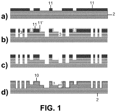
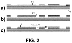
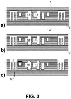
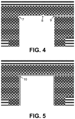
Method for Fabricating a Microfluidic Device
PatentActiveUS20210300752A1
Innovation
- A method involving direct bonding of silicon substrates with hydrophilic silicon oxide surfaces, followed by exposure to oxidative species and heat to form silicon oxide, which fills gaps and defects, enhancing fluid transport and channel sharpness.
Methods and materials for fabricating microfluidic devices
PatentInactiveEP2537657A3
Innovation
- The use of functional perfluoropolyether (PFPE) materials for fabricating microfluidic devices, which are resistant to swelling in organic solvents and feature improved chemical resistance, combined with methods for enhanced adhesion and surface functionalization to reduce bio-fouling.


Manufacturing Standards and Quality Control Requirements
The manufacturing of microfluidic devices through computational lithography demands adherence to stringent standards that ensure reproducibility, reliability, and performance consistency across production batches. International standards such as ISO 14644 for cleanroom environments and ISO 9001 for quality management systems form the foundational framework for microfluidic device fabrication. Additionally, industry-specific guidelines from organizations like the International Electrotechnical Commission (IEC) and American Society for Testing and Materials (ASTM) provide detailed specifications for semiconductor manufacturing processes that directly apply to computational lithography operations.
Critical dimensional accuracy represents a primary quality control parameter, requiring measurement tolerances within nanometer ranges for feature sizes. Advanced metrology systems including scanning electron microscopy (SEM), atomic force microscopy (AFM), and optical interferometry must be employed to verify dimensional compliance. Surface roughness specifications typically mandate Ra values below 10 nanometers to ensure proper fluid flow characteristics and minimize particle adhesion within microchannels.
Material purity standards necessitate the use of semiconductor-grade photoresists and substrates with impurity levels below parts-per-billion thresholds. Chemical composition verification through techniques such as X-ray photoelectron spectroscopy (XPS) and secondary ion mass spectrometry (SIMS) ensures material integrity throughout the fabrication process.
Process control requirements encompass real-time monitoring of critical parameters including exposure dose uniformity, development time consistency, and etching rate stability. Statistical process control (SPC) methodologies must be implemented to track process variations and maintain capability indices (Cpk) above 1.33 for critical dimensions. Environmental controls mandate temperature stability within ±0.1°C and humidity control within ±2% relative humidity during lithographic exposure operations.
Contamination control protocols require particle monitoring systems capable of detecting contaminants larger than 0.1 micrometers, with cleanroom classifications meeting ISO Class 4 or better standards. Regular calibration of all measurement equipment according to traceable standards ensures measurement accuracy and repeatability across manufacturing cycles.
Cost-Effectiveness Analysis of Computational Lithography Methods
The cost-effectiveness analysis of computational lithography methods for microfluidic device fabrication reveals significant variations across different technological approaches. Traditional photolithography, while offering high precision and established workflows, presents substantial capital expenditure requirements with equipment costs ranging from $500,000 to $2 million for advanced systems. The operational costs include expensive photomasks, specialized cleanroom facilities, and skilled technician requirements, resulting in high per-device manufacturing costs for small-batch production.
Electron beam lithography demonstrates superior resolution capabilities but suffers from extremely low throughput rates, making it economically viable only for prototype development or ultra-high-precision applications. The cost per unit area processed can be 10-50 times higher than photolithography due to sequential writing processes and extended processing times. However, its maskless nature eliminates photomask costs, providing advantages for research applications and small-volume custom designs.
Computational lithography methods, including optical proximity correction and source mask optimization, introduce additional software licensing and computational infrastructure costs. Advanced algorithms require high-performance computing resources, with software licenses ranging from $50,000 to $200,000 annually. Despite these upfront investments, computational lithography significantly reduces iteration cycles and improves yield rates, particularly for complex microfluidic geometries with sub-micron features.
Emerging techniques such as machine learning-enhanced lithography optimization show promising cost reduction potential through automated process optimization and reduced trial-and-error cycles. Initial implementation requires substantial investment in algorithm development and training datasets, but long-term benefits include reduced material waste, improved process stability, and decreased dependency on expert knowledge.
The total cost of ownership analysis indicates that computational lithography methods become increasingly cost-effective as production volumes exceed 1,000 units annually. Break-even points vary significantly based on device complexity, with simple channel geometries favoring traditional methods while complex multi-layer structures benefit from advanced computational approaches. Manufacturing scalability considerations suggest that hybrid approaches combining computational optimization with established fabrication techniques offer optimal cost-performance ratios for most commercial microfluidic applications.
Unlock deeper insights with PatSnap Eureka Quick Research — get a full tech report to explore trends and direct your research. Try now!
Generate Your Research Report Instantly with AI Agent
Supercharge your innovation with PatSnap Eureka AI Agent Platform!