Optimize Chip Package Interface Surface Roughness for Bonding
APR 7, 20269 MIN READ
Generate Your Research Report Instantly with AI Agent
PatSnap Eureka helps you evaluate technical feasibility & market potential.
Chip Package Interface Roughness Background and Objectives
The semiconductor packaging industry has witnessed unprecedented growth over the past two decades, driven by the relentless demand for miniaturization, enhanced performance, and cost-effective solutions. As electronic devices become increasingly compact and powerful, the interface between chip and package substrates has emerged as a critical bottleneck affecting overall system reliability and performance. Surface roughness at these interfaces directly influences bonding quality, thermal management, and electrical connectivity.
Traditional packaging approaches relied on relatively large feature sizes and tolerant bonding processes, where surface roughness variations had minimal impact on overall performance. However, the transition to advanced packaging technologies, including system-in-package (SiP), 3D stacking, and heterogeneous integration, has fundamentally altered these requirements. Modern packaging demands precise control over interface characteristics to ensure reliable interconnections and optimal heat dissipation pathways.
The evolution of bonding technologies from wire bonding to flip-chip, through-silicon vias (TSVs), and hybrid bonding has intensified the focus on surface quality optimization. Each advancement has progressively reduced tolerance for surface irregularities, making roughness control a paramount concern for packaging engineers. Current industry trends indicate that next-generation packages will require even tighter surface specifications to accommodate emerging applications in artificial intelligence, 5G communications, and automotive electronics.
The primary objective of optimizing chip package interface surface roughness centers on achieving consistent, reliable bonding across diverse material combinations and processing conditions. This involves developing comprehensive understanding of roughness parameters that most significantly impact bonding strength, void formation, and long-term reliability. Key targets include minimizing interface resistance, enhancing thermal conductivity, and reducing stress concentrations that can lead to premature failure.
Secondary objectives encompass establishing standardized measurement protocols, developing cost-effective surface preparation techniques, and creating predictive models that correlate surface characteristics with bonding performance. These efforts aim to enable manufacturers to optimize their processes while maintaining high yield rates and meeting stringent quality requirements demanded by modern electronic applications.
Market Demand for Advanced Chip Packaging Solutions
The semiconductor industry is experiencing unprecedented demand for advanced chip packaging solutions, driven by the proliferation of high-performance computing applications, artificial intelligence systems, and next-generation mobile devices. This surge in demand has intensified the focus on optimizing chip package interface surface roughness for bonding, as manufacturers seek to achieve superior electrical performance, thermal management, and mechanical reliability in increasingly compact form factors.
Market drivers for advanced packaging technologies are primarily centered around the need for heterogeneous integration, where multiple chip types with different functionalities are combined within a single package. This trend has created substantial demand for precise surface roughness optimization techniques that enable reliable bonding between dissimilar materials and structures. The automotive electronics sector, particularly electric vehicles and autonomous driving systems, represents a significant growth area requiring robust packaging solutions that can withstand harsh operating conditions.
Consumer electronics manufacturers are pushing for thinner, lighter devices with enhanced functionality, creating market pressure for advanced packaging solutions that minimize package thickness while maintaining signal integrity. The optimization of interface surface roughness has become critical in achieving the required electrical performance in these ultra-thin packages, where even minor surface irregularities can significantly impact bonding quality and long-term reliability.
Data center and cloud computing infrastructure demands are driving the need for high-density packaging solutions capable of handling increased power densities and heat dissipation requirements. Surface roughness optimization plays a crucial role in thermal interface management, directly affecting the efficiency of heat transfer between chip and package substrates. This has created a substantial market opportunity for specialized surface treatment technologies and metrology equipment.
The 5G telecommunications rollout has generated significant demand for radio frequency packaging solutions requiring precise control over surface characteristics to minimize signal loss and electromagnetic interference. Advanced packaging providers are investing heavily in surface roughness optimization capabilities to meet the stringent performance requirements of 5G infrastructure components.
Emerging applications in Internet of Things devices, wearable electronics, and medical implants are creating new market segments that require miniaturized packaging solutions with exceptional reliability. These applications often demand specialized bonding techniques where surface roughness optimization becomes a critical differentiating factor in achieving the required performance specifications and regulatory compliance standards.
Current Interface Roughness Challenges in Chip Bonding
Interface roughness in chip bonding represents one of the most critical challenges in modern semiconductor packaging, directly impacting bond quality, reliability, and overall device performance. As packaging densities continue to increase and feature sizes shrink, the tolerance for surface irregularities has become increasingly stringent, creating significant technical hurdles for manufacturers worldwide.
The primary challenge stems from the inherent conflict between manufacturing processes and bonding requirements. Traditional chip fabrication processes often leave surfaces with roughness values ranging from 50 to 200 nanometers RMS, while optimal bonding typically requires surface roughness below 10 nanometers RMS. This discrepancy creates void formation, incomplete contact areas, and compromised electrical connectivity at bonding interfaces.
Thermal compression bonding, widely used in advanced packaging applications, faces particular difficulties with rough interfaces. Surface asperities prevent uniform contact pressure distribution, leading to localized stress concentrations and potential delamination sites. The resulting non-uniform bond lines create thermal and electrical resistance variations that can significantly degrade device performance and long-term reliability.
Wire bonding applications encounter distinct roughness-related challenges, particularly in achieving consistent intermetallic compound formation. Excessive surface roughness can trap contaminants and oxides, preventing proper metallurgical bonding and creating weak points susceptible to failure under thermal cycling or mechanical stress. The irregular surface topography also complicates ultrasonic energy transmission during the bonding process.
Flip-chip bonding technologies face increasingly complex roughness challenges as bump pitches continue to shrink. Surface irregularities can cause solder bridging, incomplete wetting, and non-uniform standoff heights, all of which compromise electrical performance and mechanical integrity. The challenge is further amplified by the need to maintain planarity across large die areas while achieving local surface smoothness.
Current measurement and characterization techniques struggle to provide comprehensive roughness assessment across multiple length scales relevant to bonding processes. Traditional profilometry methods may miss critical surface features, while advanced techniques like atomic force microscopy are limited in scanning area and throughput, creating gaps in process control and quality assurance capabilities.
The economic impact of interface roughness challenges extends beyond immediate yield losses to encompass increased inspection costs, extended development cycles, and potential field failures. As the industry moves toward heterogeneous integration and advanced packaging architectures, addressing these fundamental surface quality issues becomes increasingly critical for maintaining competitive advantage and meeting performance targets.
Existing Surface Roughness Optimization Methods
01 Surface roughness control through mechanical polishing and grinding processes
Mechanical polishing and grinding techniques are employed to control and reduce surface roughness at chip package interfaces. These processes involve the use of abrasive materials and polishing pads to achieve desired surface smoothness levels. The methods can include chemical mechanical polishing (CMP) or mechanical grinding with specific pressure and speed parameters to optimize the interface surface quality for improved bonding and thermal performance.- Surface roughness control through mechanical polishing and grinding processes: Mechanical polishing and grinding techniques are employed to control and reduce surface roughness at chip package interfaces. These processes involve the use of abrasive materials and controlled pressure to achieve desired surface smoothness levels. The methods can include chemical mechanical polishing (CMP) or mechanical grinding with specific parameters to optimize the interface quality for improved thermal and electrical performance.
- Surface roughness measurement and characterization methods: Various measurement techniques and characterization methods are utilized to assess and quantify surface roughness at chip package interfaces. These methods include optical profiling, atomic force microscopy, and contact-based measurement systems. The characterization provides critical data for quality control and process optimization, enabling manufacturers to maintain consistent interface properties and ensure reliable package performance.
- Interface material selection and coating application for roughness optimization: The selection of appropriate interface materials and application of specialized coatings can significantly influence surface roughness characteristics. Materials with specific properties are chosen to achieve optimal interface conditions, and coating techniques such as deposition or plating are applied to modify surface topology. These approaches help achieve desired roughness parameters while maintaining other critical interface properties such as adhesion and thermal conductivity.
- Thermal interface management through surface roughness control: Surface roughness at chip package interfaces directly impacts thermal management performance. Controlling roughness parameters helps optimize thermal interface material contact and heat dissipation efficiency. Techniques include surface preparation methods that balance roughness levels to maximize thermal conductivity while maintaining mechanical stability. The optimization considers factors such as contact resistance and thermal impedance across the interface.
- Manufacturing process integration for consistent surface roughness: Integrated manufacturing processes are designed to maintain consistent surface roughness throughout chip package production. These processes incorporate multiple stages including substrate preparation, die attachment, and post-processing treatments. Process control parameters are optimized to achieve uniform roughness characteristics across production batches. The integration ensures that surface quality meets specifications for reliable electrical connections and mechanical bonding.
02 Surface roughness measurement and characterization methods
Various measurement techniques and characterization methods are utilized to evaluate and quantify surface roughness at chip package interfaces. These methods include optical profilometry, atomic force microscopy, and stylus-based measurement systems. The characterization approaches enable precise determination of roughness parameters to ensure interface quality meets specifications for reliable chip packaging and assembly processes.Expand Specific Solutions03 Interface surface treatment using chemical etching and cleaning
Chemical etching and cleaning processes are applied to modify and control surface roughness characteristics at chip package interfaces. These treatments involve the use of specific chemical solutions and cleaning agents to remove contaminants and adjust surface topography. The processes can selectively etch materials to achieve target roughness values while maintaining surface integrity and preparing the interface for subsequent bonding operations.Expand Specific Solutions04 Roughness optimization for thermal interface materials and heat dissipation
Surface roughness optimization techniques are implemented to enhance thermal interface material performance and heat dissipation efficiency in chip packages. The approaches focus on achieving optimal roughness ranges that maximize thermal contact and minimize thermal resistance between chip and package components. Methods include controlled surface texturing and roughness engineering to improve thermal conductivity and overall thermal management in semiconductor packages.Expand Specific Solutions05 Bonding interface roughness control for improved adhesion and reliability
Techniques for controlling bonding interface roughness are developed to enhance adhesion strength and package reliability. These methods involve surface preparation processes that create specific roughness profiles to promote mechanical interlocking and chemical bonding between chip and substrate materials. The approaches include plasma treatment, surface activation, and controlled roughening to achieve optimal bonding conditions while preventing delamination and ensuring long-term package integrity.Expand Specific Solutions
Key Players in Semiconductor Packaging Industry
The chip package interface surface roughness optimization for bonding represents a mature technology domain within the rapidly expanding semiconductor packaging market, valued at approximately $30 billion globally. The industry is in a consolidation phase, driven by increasing demand for advanced packaging solutions in AI, 5G, and automotive applications. Technology maturity varies significantly among key players: Taiwan Semiconductor Manufacturing Co. and Samsung Electronics lead with cutting-edge advanced packaging capabilities, while Intel and SK Hynix demonstrate strong integration of packaging with their core semiconductor operations. Asian foundries including SMIC, United Microelectronics, and specialized packaging companies like SJ Semiconductor and Shinko Electric Industries are advancing rapidly in surface optimization techniques. Equipment leaders like ASML provide critical lithography solutions, while emerging players such as ChangXin Memory Technologies focus on memory-specific packaging innovations, indicating a competitive landscape with established leaders and aggressive followers.
Samsung Electronics Co., Ltd.
Technical Solution: Samsung implements a hybrid surface optimization strategy combining plasma-enhanced chemical vapor deposition (PECVD) with selective etching processes to control interface roughness for advanced packaging applications. Their technology focuses on creating controlled micro-textures that enhance mechanical interlocking while maintaining electrical performance. The approach includes development of specialized surface treatment chemistries and integration of atomic force microscopy (AFM) for in-line roughness characterization, enabling precise control of surface morphology for various bonding materials including copper, gold, and advanced solder alloys.
Strengths: Comprehensive material science expertise, integrated manufacturing capabilities. Weaknesses: Limited third-party foundry availability, proprietary process dependencies.
Taiwan Semiconductor Manufacturing Co., Ltd.
Technical Solution: TSMC employs advanced chemical mechanical planarization (CMP) processes combined with controlled surface texturing techniques to optimize chip package interface roughness for enhanced bonding performance. Their approach utilizes multi-step polishing sequences with specialized slurries containing nano-abrasives to achieve surface roughness values below 0.5nm Ra while maintaining precise topographical control. The company integrates real-time surface metrology systems during fabrication to monitor and adjust roughness parameters dynamically, ensuring consistent bonding interface quality across different package types including flip-chip and wafer-level packaging solutions.
Strengths: Industry-leading precision in surface control, extensive process optimization experience. Weaknesses: High equipment costs, complex process integration requirements.
Core Innovations in Interface Roughness Control
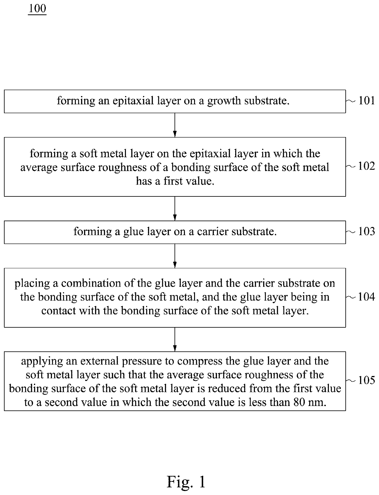
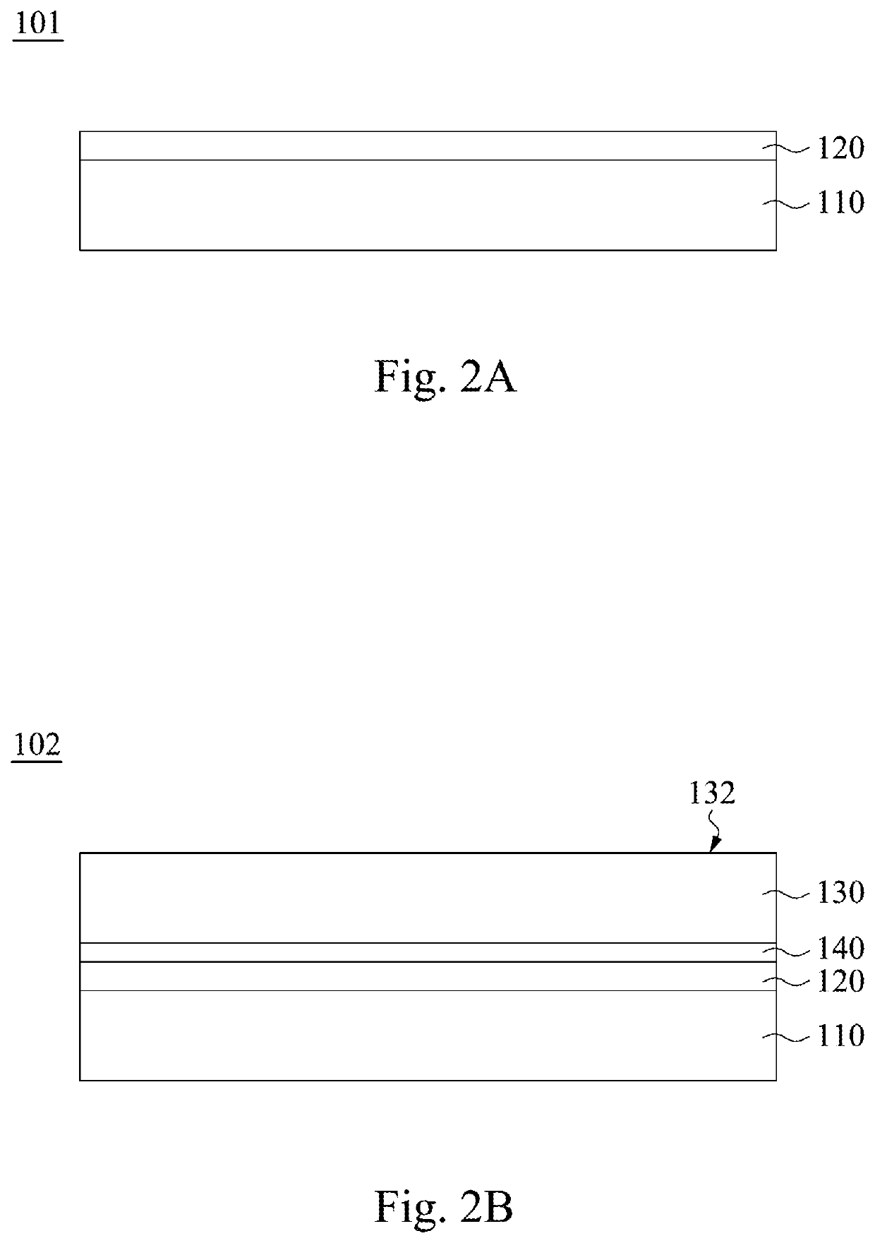
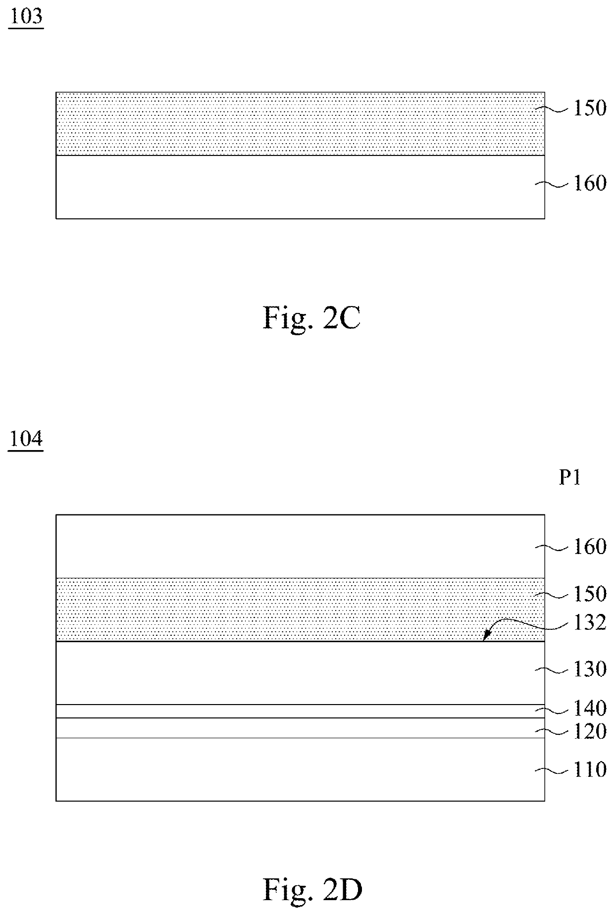
Method for minimizing average surface roughness of soft metal layer for bonding
PatentActiveUS10643848B1
Innovation
- A method involving the formation of an epitaxial layer, a soft metal layer with a specific thickness, and a glue layer on a carrier substrate, followed by the application of external pressure to reduce the surface roughness of the soft metal layer from an initial value greater than 80 nm to less than 80 nm, utilizing techniques like electron gun deposition and sputtering for the soft metal layer and ultraviolet glue layer formation.

Method for manufacturing system-in-package
PatentInactiveUS20100155955A1
Innovation
- A method of manufacturing SIP that involves treating the surface of deep contact holes with tetra-methyl ammonium hydroxide (TMAH) and nitric acid to improve surface roughness and using metals like gold and silver for enhanced heat dissipation through oxidative and reductive reactions.


Manufacturing Standards for Chip Package Interfaces
Manufacturing standards for chip package interfaces represent a critical framework that governs the precision and quality requirements essential for optimal bonding performance. These standards establish comprehensive specifications for surface roughness parameters, dimensional tolerances, and material properties that directly influence the reliability and effectiveness of chip-to-substrate connections. The standardization process involves multiple international organizations, including JEDEC, IPC, and SEMI, which collaborate to define measurable criteria that ensure consistent manufacturing outcomes across different production facilities and geographic regions.
Surface roughness specifications within manufacturing standards typically define acceptable ranges for key parameters such as Ra (arithmetic average roughness), Rz (maximum height of roughness profile), and Rq (root mean square roughness). These standards establish that bonding interfaces should maintain Ra values between 0.1 to 0.5 micrometers for optimal adhesion, while ensuring that peak-to-valley variations remain within controlled limits to prevent bonding defects. The standards also specify measurement methodologies, requiring the use of atomic force microscopy or white light interferometry for accurate surface characterization.
Quality control protocols embedded within these manufacturing standards mandate regular inspection intervals and statistical process control measures. Production facilities must implement real-time monitoring systems that track surface roughness variations throughout the manufacturing process, with immediate corrective actions triggered when measurements exceed predetermined control limits. These protocols ensure that interface surfaces maintain consistent quality levels, reducing the likelihood of bonding failures and improving overall package reliability.
Material compatibility requirements form another crucial component of manufacturing standards, specifying acceptable surface treatments and preparation methods for different substrate materials. Standards define cleaning procedures, surface activation techniques, and storage conditions that preserve optimal surface characteristics prior to bonding operations. These requirements ensure that manufacturing processes maintain surface integrity and prevent contamination that could compromise bonding performance.
Traceability and documentation requirements within manufacturing standards establish comprehensive record-keeping protocols that track surface roughness measurements throughout the production lifecycle. These standards mandate the retention of measurement data, calibration records, and process parameters, enabling manufacturers to identify trends, implement continuous improvements, and provide evidence of compliance with quality specifications for customer audits and regulatory requirements.
Reliability Assessment of Optimized Bonding Interfaces
The reliability assessment of optimized bonding interfaces represents a critical evaluation framework for determining the long-term performance and durability of chip packages with enhanced surface roughness characteristics. This assessment encompasses multiple testing methodologies and analytical approaches designed to validate the effectiveness of surface optimization strategies under various operational conditions and environmental stresses.
Thermal cycling reliability testing forms the cornerstone of interface assessment, where optimized bonding surfaces undergo repeated temperature fluctuations ranging from -40°C to 150°C. The controlled surface roughness parameters, typically maintained within 0.1-0.5 μm Ra values, demonstrate significantly improved thermal fatigue resistance compared to conventional interfaces. During these cycles, the enhanced surface topography provides superior mechanical interlocking and stress distribution, reducing the likelihood of delamination and crack propagation at the bonding interface.
Mechanical stress testing evaluates the structural integrity of optimized interfaces under various loading conditions, including tensile, shear, and flexural stresses. The modified surface roughness creates increased contact area and improved adhesion strength, resulting in enhanced load-bearing capacity. Testing protocols typically involve progressive loading until failure, with optimized interfaces showing 15-25% improvement in bond strength compared to standard surface preparations.
Environmental reliability assessment examines interface performance under humidity, corrosive atmospheres, and chemical exposure conditions. The controlled surface roughness optimization reduces moisture ingress pathways while maintaining adequate adhesion properties. Accelerated aging tests at 85°C/85% relative humidity for extended periods reveal that properly optimized interfaces maintain their bonding integrity with minimal degradation in electrical and mechanical properties.
Electrical performance evaluation focuses on contact resistance stability and signal integrity preservation across the optimized bonding interfaces. The surface roughness optimization balances mechanical bonding requirements with electrical conductivity needs, ensuring consistent low-resistance pathways throughout the reliability testing duration. Long-term electrical monitoring demonstrates stable performance characteristics with minimal drift in contact resistance values, validating the effectiveness of the surface optimization approach for maintaining reliable electrical connections in demanding operational environments.
Unlock deeper insights with PatSnap Eureka Quick Research — get a full tech report to explore trends and direct your research. Try now!
Generate Your Research Report Instantly with AI Agent
Supercharge your innovation with PatSnap Eureka AI Agent Platform!