

Photodiode evolution in precision scientific observation devices
AUG 21, 20259 MIN READ
Generate Your Research Report Instantly with AI Agent
PatSnap Eureka helps you evaluate technical feasibility & market potential.
Photodiode Tech Evolution
The evolution of photodiodes in precision scientific observation devices has been marked by significant advancements in sensitivity, speed, and reliability. Initially developed in the early 20th century, photodiodes have undergone a remarkable transformation, driven by the increasing demands of scientific research and technological applications.
In the 1950s and 1960s, silicon photodiodes emerged as a major breakthrough, offering improved quantum efficiency and broader spectral response compared to their selenium and germanium predecessors. This development paved the way for more accurate light detection in various scientific instruments, including spectrophotometers and radiation detectors.
The 1970s and 1980s saw the introduction of PIN (Positive-Intrinsic-Negative) photodiodes, which featured an intrinsic layer between the p and n regions. This structure significantly enhanced the device's speed and sensitivity, making it ideal for high-precision measurements in fields such as laser rangefinding and fiber-optic communications.
Avalanche photodiodes (APDs) marked another milestone in the 1990s. These devices utilized internal gain mechanisms to amplify weak light signals, enabling detection of extremely low light levels. APDs found extensive applications in areas like quantum cryptography and LIDAR systems for atmospheric studies.
The turn of the millennium brought about the development of single-photon avalanche diodes (SPADs). These ultra-sensitive devices could detect individual photons, revolutionizing quantum optics experiments and enabling advancements in fields such as fluorescence microscopy and quantum computing.
Recent years have witnessed the emergence of novel materials and structures in photodiode technology. For instance, graphene-based photodetectors have shown promise in achieving ultra-broadband detection, spanning from ultraviolet to terahertz frequencies. Additionally, the integration of nanostructures, such as quantum dots and nanowires, has led to photodiodes with enhanced light absorption and carrier collection efficiency.
The ongoing miniaturization trend has resulted in the development of highly compact photodiode arrays and integrated photonic circuits. These advancements have enabled the creation of sophisticated imaging systems and spectroscopic devices with unprecedented spatial and temporal resolution, crucial for applications in astronomy, medical diagnostics, and environmental monitoring.
Market Demand Analysis
The market demand for photodiodes in precision scientific observation devices has been experiencing significant growth, driven by advancements in various scientific fields and the increasing need for high-precision measurements. This demand is particularly evident in sectors such as astronomy, particle physics, medical imaging, and environmental monitoring.
In the field of astronomy, the evolution of photodiodes has enabled more sensitive and accurate detection of faint light sources, crucial for studying distant celestial objects and phenomena. Large-scale projects like the Large Synoptic Survey Telescope (LSST) and the James Webb Space Telescope rely heavily on advanced photodiode technology for their imaging capabilities. This has created a substantial market for high-performance photodiodes capable of operating in extreme conditions with minimal noise.
The particle physics sector has also been a major driver of photodiode demand, particularly in applications such as scintillation detectors used in high-energy physics experiments. The ongoing upgrades to facilities like CERN's Large Hadron Collider require increasingly sophisticated photodiode arrays for particle detection and measurement, further expanding the market.
In medical imaging, the demand for photodiodes has been fueled by the growing adoption of positron emission tomography (PET) scanners and other advanced diagnostic tools. These devices require highly sensitive photodiodes to detect the gamma rays produced during radioactive decay, enabling more accurate and detailed imaging of biological processes.
Environmental monitoring applications have also contributed to the expanding market for precision photodiodes. From atmospheric research to ocean exploration, scientists are increasingly relying on photodiode-based sensors to measure light levels, detect pollutants, and monitor climate change indicators with unprecedented accuracy.
The market for photodiodes in scientific observation devices is expected to continue its upward trajectory, with a particular focus on improving sensitivity, reducing noise, and enhancing durability. Manufacturers are investing in research and development to produce photodiodes with higher quantum efficiency, faster response times, and broader spectral ranges to meet the evolving needs of the scientific community.
As governments and private institutions increase their investments in scientific research and exploration, the demand for cutting-edge observation devices equipped with advanced photodiodes is likely to grow. This trend is further supported by the increasing emphasis on data-driven decision-making across various scientific disciplines, which requires more precise and reliable measurement tools.
Current Challenges
The evolution of photodiodes in precision scientific observation devices faces several significant challenges that hinder their further advancement and widespread application. One of the primary obstacles is the persistent issue of dark current, which introduces noise and limits the sensitivity of these devices, especially in low-light conditions. Despite ongoing efforts to mitigate this problem, achieving ultra-low dark current levels remains a formidable task, particularly for large-area photodiodes required in certain scientific applications.
Another critical challenge lies in improving the quantum efficiency of photodiodes across a broader spectral range. While significant progress has been made in enhancing sensitivity within specific wavelength bands, extending high quantum efficiency uniformly across the entire spectrum from ultraviolet to near-infrared remains elusive. This limitation restricts the versatility of photodiodes in multi-spectral scientific observations.
The trade-off between speed and sensitivity continues to pose a significant challenge for researchers and engineers. High-speed photodiodes often sacrifice sensitivity, while highly sensitive devices typically operate at lower speeds. Striking an optimal balance between these two crucial parameters is essential for advancing the capabilities of precision scientific instruments, particularly in applications requiring both rapid response and high sensitivity.
Miniaturization of photodiodes while maintaining or improving their performance characteristics presents another hurdle. As scientific instruments become more compact and portable, there is a growing demand for smaller photodiodes that do not compromise on sensitivity, speed, or spectral response. This challenge is particularly acute in space-based observations and portable scientific equipment.
The integration of photodiodes with readout electronics and signal processing circuits poses significant challenges in terms of noise reduction and signal integrity. As the performance of photodiodes improves, the associated electronics must evolve to match this progress, necessitating advancements in low-noise amplifiers, analog-to-digital converters, and on-chip signal processing capabilities.
Radiation hardness remains a critical concern for photodiodes used in space-based scientific instruments and other high-radiation environments. Developing photodiodes that can maintain their performance characteristics under prolonged exposure to cosmic rays and other forms of ionizing radiation continues to be a significant challenge, requiring innovative materials and device architectures.
Lastly, the cost-effective production of high-performance photodiodes at scale presents a substantial challenge. Many advanced photodiode technologies that show promise in laboratory settings face difficulties in transitioning to large-scale manufacturing processes. Bridging this gap between research prototypes and commercially viable products is crucial for the widespread adoption of next-generation photodiodes in precision scientific observation devices.
Existing Solutions
01 Improved photodiode structure for enhanced precision
Advanced photodiode structures are designed to improve precision by optimizing light absorption and reducing noise. These structures may include specialized doping profiles, novel materials, or unique geometries that enhance sensitivity and reduce dark current.- Improved photodiode structure for enhanced precision: Advanced photodiode structures are designed to improve precision by optimizing light absorption and reducing noise. These structures may include specialized doping profiles, novel materials, or unique geometries that enhance sensitivity and reduce dark current. Such improvements allow for more accurate light detection and measurement in various applications.
- Integration of photodiodes with readout circuits: Integrating photodiodes with readout circuits on the same chip can significantly improve precision by reducing noise and parasitic effects. This approach allows for better signal processing, faster response times, and improved overall system performance. The integration may involve CMOS technology or other semiconductor fabrication techniques to create compact and efficient photodetector systems.
- Temperature compensation techniques for photodiodes: Temperature variations can affect photodiode performance and precision. Implementing temperature compensation techniques, such as using temperature sensors, feedback loops, or specialized circuit designs, can help maintain consistent photodiode output across different operating temperatures. This approach ensures high precision in various environmental conditions.
- Avalanche photodiodes for high-sensitivity applications: Avalanche photodiodes (APDs) offer high internal gain and improved sensitivity for low-light applications. These devices utilize impact ionization to amplify the photocurrent, resulting in enhanced precision for weak signal detection. APDs are particularly useful in applications requiring high-speed, high-sensitivity photodetection.
- Novel materials and fabrication techniques for photodiodes: Exploring new materials and fabrication techniques can lead to improved photodiode precision. This may include using compound semiconductors, nanostructures, or advanced deposition methods to create photodiodes with superior optical and electrical properties. These innovations can result in devices with higher quantum efficiency, lower noise, and better overall performance.
02 Integration of precision circuitry with photodiodes
Precision circuitry is integrated with photodiodes to enhance overall performance. This may include on-chip amplifiers, analog-to-digital converters, or signal processing units that work in conjunction with the photodiode to improve accuracy and reduce noise.Expand Specific Solutions03 Temperature compensation techniques for photodiodes
Various methods are employed to compensate for temperature-induced variations in photodiode performance. These may include integrated temperature sensors, bias control circuits, or algorithmic corrections to maintain precision across a wide temperature range.Expand Specific Solutions04 Specialized packaging and shielding for precision photodiodes
Advanced packaging and shielding techniques are used to protect precision photodiodes from external interference and environmental factors. This may include hermetic sealing, electromagnetic shielding, or specialized optical coatings to enhance performance and longevity.Expand Specific Solutions05 Calibration and self-testing mechanisms for photodiodes
Innovative calibration and self-testing mechanisms are incorporated into photodiode systems to ensure ongoing precision. These may include built-in light sources for periodic calibration, self-diagnostic routines, or adaptive algorithms that maintain accuracy over time.Expand Specific Solutions
Key Industry Players
The photodiode evolution in precision scientific observation devices is in a mature yet dynamic phase, with ongoing advancements driven by key industry players. The market size is substantial, reflecting the critical role of photodiodes in various scientific and industrial applications. Companies like Sony Semiconductor Solutions, Samsung Electronics, and STMicroelectronics are at the forefront, leveraging their extensive R&D capabilities to push the boundaries of photodiode technology. The competitive landscape is characterized by a mix of established electronics giants and specialized firms like OSI Optoelectronics and SiliconFile Technologies, each contributing to incremental improvements in sensitivity, speed, and integration capabilities of photodiodes for high-precision scientific instruments.
Sony Semiconductor Solutions Corp.
Technical Solution: Sony has developed advanced stacked CMOS image sensors with high-speed global shutter function for precision scientific observation. Their technology incorporates a pixel-parallel analog-to-digital converter (ADC) and digital memory for each pixel, enabling high-speed readout and reduced noise[1]. The company has also introduced back-illuminated time-of-flight (ToF) image sensors with 4-tap avalanche photodiodes, which significantly improve distance measurement accuracy and speed for various scientific applications[2]. Sony's photodiodes feature a unique copper-to-copper bonding technology that allows for miniaturization while maintaining high performance[3].
Strengths: High-speed readout, reduced noise, improved distance measurement accuracy. Weaknesses: Potentially higher cost due to advanced manufacturing processes, may require specialized integration.
Raytheon Co.
Technical Solution: Raytheon has developed high-performance avalanche photodiodes (APDs) for precision scientific observation devices. Their APDs feature a unique separate absorption and multiplication (SAM) structure, which allows for optimization of both the absorption and multiplication regions independently[4]. This results in improved sensitivity and lower noise compared to traditional APD designs. Raytheon's photodiodes also incorporate advanced passivation techniques to reduce surface leakage currents and improve reliability[5]. The company has demonstrated APDs with high quantum efficiency (>80%) across a wide spectral range, making them suitable for various scientific applications, including LIDAR and spectroscopy[6].
Strengths: High sensitivity, low noise, wide spectral range. Weaknesses: Potentially higher complexity in manufacturing, may require cooling for optimal performance in some applications.
Core Innovations
Avalanche photodiode
PatentActiveUS20080067620A1
Innovation
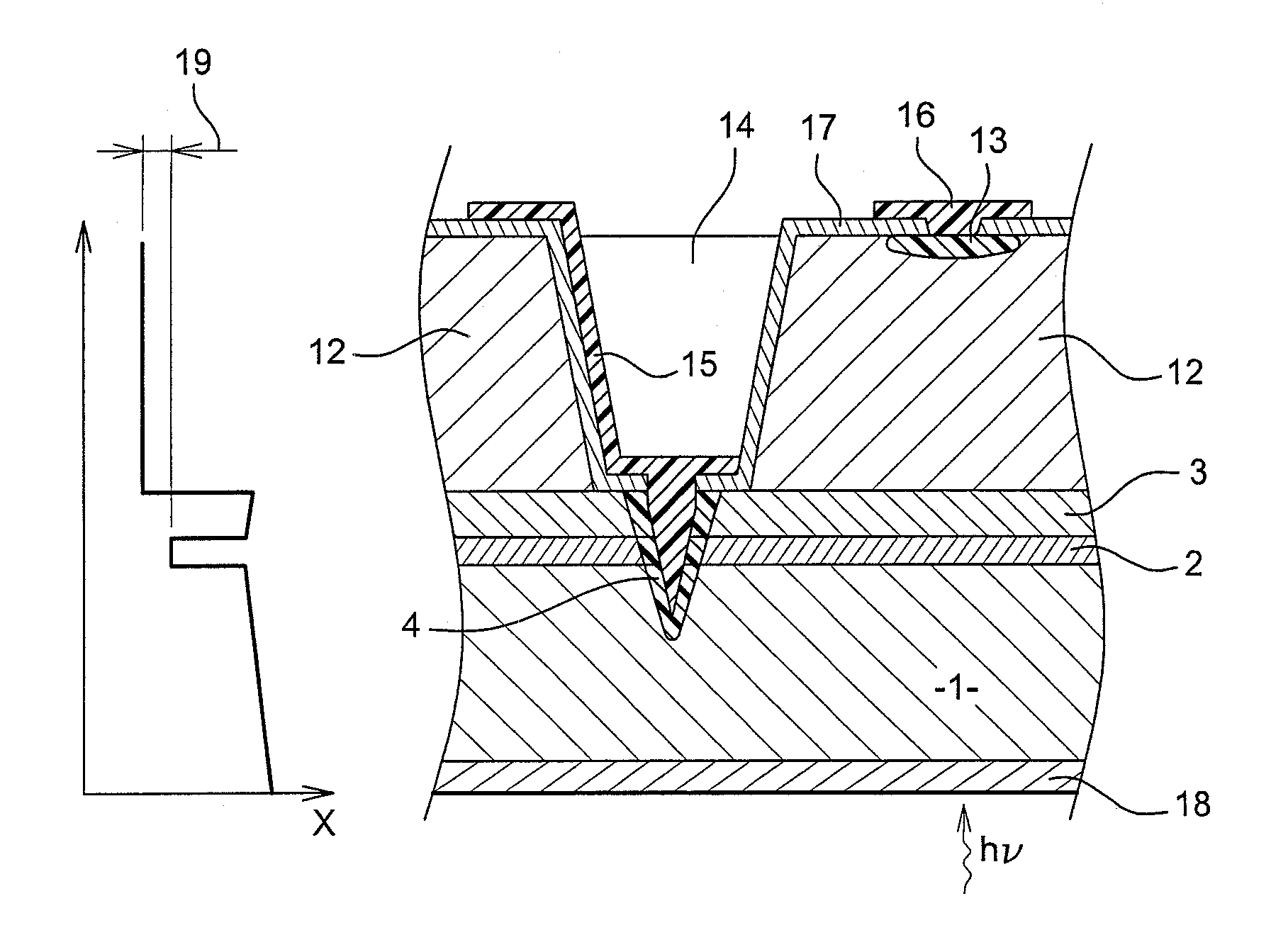
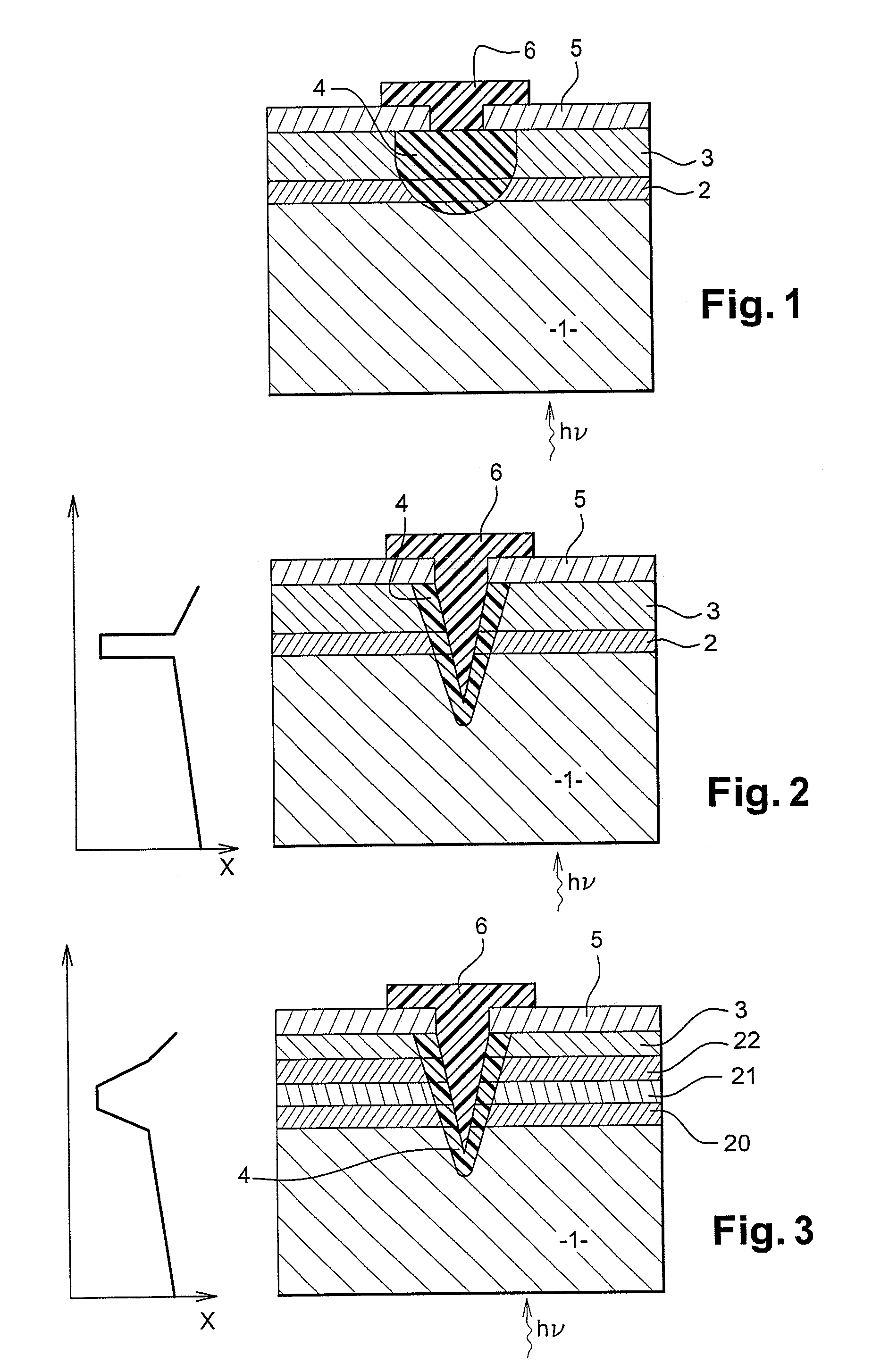
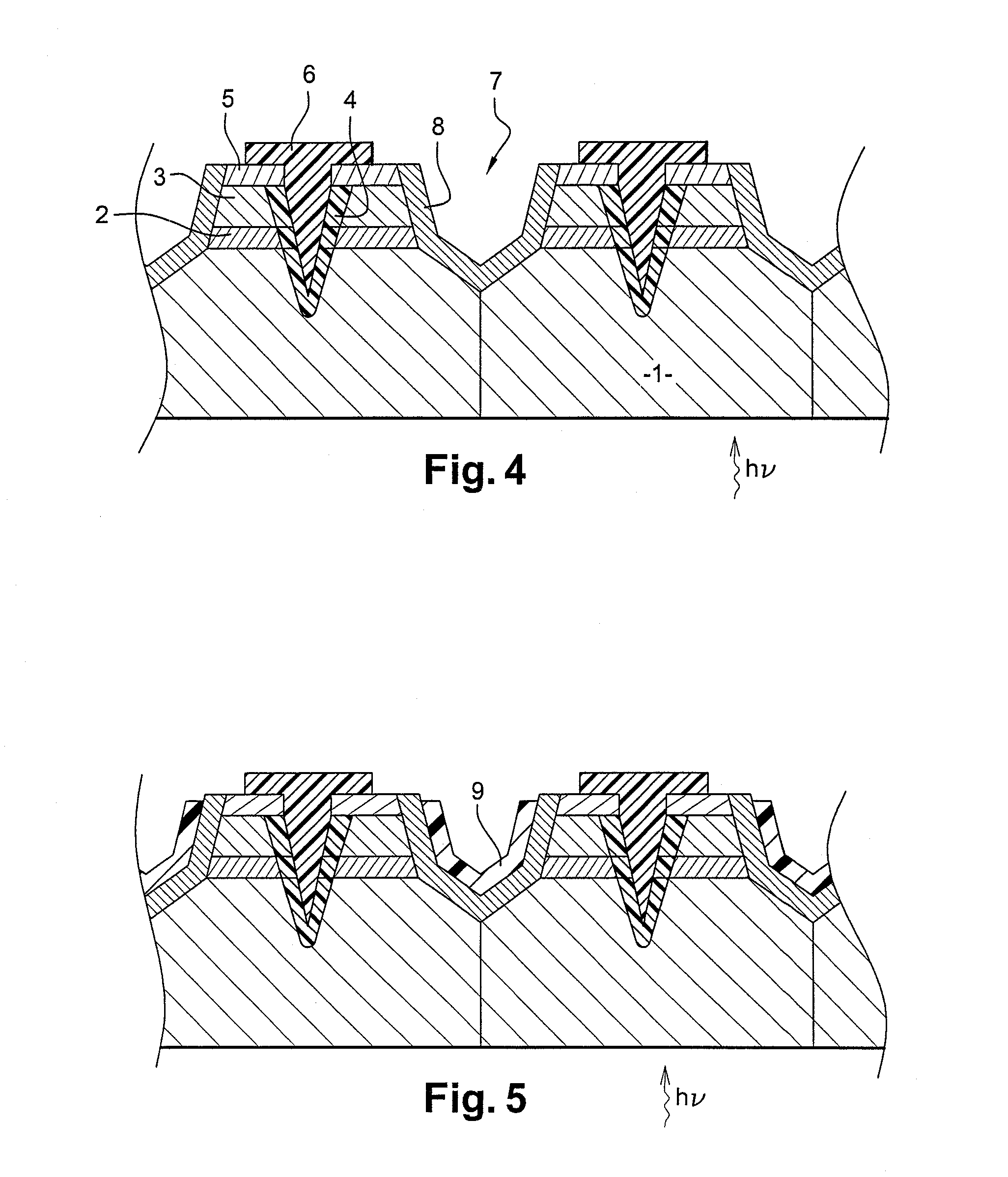
- A photodiode structure comprising a stack of semiconductor layers with a collection layer thinner than the interaction layer, a confinement layer with a larger band gap, and a transverse region forming a p-n junction, optimized with a band gap gradient and passivation layers to minimize noise and dark current, allowing high gain with low reverse bias without degrading the signal-to-noise ratio.

A radiation detector having a bandgap engineered absorber
PatentInactiveEP2284895A2
Innovation
- A radiation detector with a photodiode featuring a graded multilayer absorber structure, where multiple semiconductor layers with varying bandgaps are used to confine the longer cutoff region to a thin layer, reducing dark current and allowing operation at higher temperatures without performance degradation.


Regulatory Landscape
The regulatory landscape surrounding photodiodes in precision scientific observation devices has evolved significantly over the years, reflecting the increasing importance of these components in various fields. Regulatory bodies across different regions have established stringent standards to ensure the reliability, accuracy, and safety of photodiode-based instruments.
In the United States, the Food and Drug Administration (FDA) plays a crucial role in regulating photodiodes used in medical devices. The FDA's Center for Devices and Radiological Health (CDRH) oversees the approval process for devices incorporating photodiodes, ensuring they meet safety and efficacy standards. Similarly, the European Union has implemented the Medical Device Regulation (MDR), which includes specific requirements for photodiode-based medical equipment.
For environmental monitoring applications, agencies such as the Environmental Protection Agency (EPA) in the United States and the European Environment Agency (EEA) have set guidelines for the use of photodiodes in air quality monitoring instruments. These regulations often specify minimum detection limits, response times, and calibration procedures to ensure accurate and consistent measurements.
In the aerospace sector, organizations like NASA and ESA have established rigorous standards for photodiodes used in space-based observation instruments. These regulations address issues such as radiation hardness, thermal stability, and long-term reliability in the harsh space environment.
The International Electrotechnical Commission (IEC) has developed several standards specifically for photodiodes, including IEC 60747-5-3 for discrete devices and IEC 60747-5-5 for arrays. These standards define terminology, measurement methods, and performance criteria, providing a common framework for manufacturers and users worldwide.
As the applications of photodiodes in precision scientific instruments continue to expand, regulatory bodies are adapting their frameworks to address emerging technologies. For instance, the increasing use of avalanche photodiodes (APDs) and single-photon avalanche diodes (SPADs) in quantum sensing and communication has prompted the development of new standards and guidelines.
Compliance with these regulations often requires extensive documentation, testing, and certification processes. Manufacturers must demonstrate that their photodiode-based devices meet the specified performance criteria and safety requirements. This regulatory landscape not only ensures the quality and reliability of scientific instruments but also drives innovation as companies strive to develop photodiodes that exceed regulatory standards.
Environmental Impact
The evolution of photodiodes in precision scientific observation devices has significant environmental implications. These devices, increasingly utilized in various scientific fields, contribute to our understanding of environmental phenomena and climate change. As photodiodes become more sensitive and efficient, they enable more accurate measurements of light intensity, spectral composition, and other optical properties, enhancing our ability to monitor and analyze environmental conditions.
The improved performance of photodiodes has led to the development of more compact and energy-efficient scientific instruments. This reduction in size and power consumption translates to decreased environmental impact during manufacturing, transportation, and operation. Additionally, the longevity and reliability of modern photodiodes contribute to the extended lifespan of scientific devices, reducing electronic waste and the need for frequent replacements.
In environmental monitoring applications, advanced photodiodes play a crucial role in detecting and measuring pollutants, greenhouse gases, and other atmospheric components. This enhanced capability supports more effective environmental protection strategies and policy-making. For instance, satellite-based instruments equipped with high-performance photodiodes provide valuable data on global climate patterns, deforestation, and ocean health.
The integration of photodiodes in precision scientific devices has also facilitated the development of renewable energy technologies. Improved solar cell efficiency, enabled by advanced photodiode technology, contributes to the growth of clean energy sources and the reduction of fossil fuel dependence. Furthermore, photodiodes are essential components in light detection and ranging (LiDAR) systems used for mapping forests, monitoring ice sheets, and studying ecosystem dynamics.
However, the production of high-performance photodiodes often involves rare earth elements and specialized manufacturing processes, which can have environmental consequences. The extraction and processing of these materials may lead to habitat disruption and pollution if not managed responsibly. As the demand for precision scientific devices grows, it becomes increasingly important to develop sustainable manufacturing practices and explore eco-friendly alternatives for photodiode production.
In conclusion, while the evolution of photodiodes in precision scientific observation devices has largely positive environmental impacts through improved monitoring capabilities and energy efficiency, it also presents challenges related to resource extraction and manufacturing. Balancing these factors is crucial for ensuring that the advancement of scientific instrumentation aligns with broader environmental sustainability goals.
Unlock deeper insights with PatSnap Eureka Quick Research — get a full tech report to explore trends and direct your research. Try now!
Generate Your Research Report Instantly with AI Agent
Supercharge your innovation with PatSnap Eureka AI Agent Platform!