Advances in photodiode component compatibility in research setups
AUG 21, 20259 MIN READ
Generate Your Research Report Instantly with AI Agent
Patsnap Eureka helps you evaluate technical feasibility & market potential.
Photodiode Advancements
Photodiode technology has undergone significant advancements in recent years, particularly in terms of component compatibility within research setups. These improvements have been driven by the increasing demand for more precise and versatile light detection systems across various scientific disciplines.
One of the key areas of progress has been in the development of photodiodes with enhanced spectral responsivity. Modern photodiodes now offer broader wavelength detection ranges, allowing researchers to capture and analyze light across a wider spectrum. This expanded capability has proven invaluable in fields such as spectroscopy, where the ability to detect subtle variations in light emission is crucial.
Another notable advancement is the miniaturization of photodiode components. Manufacturers have successfully reduced the size of photodiodes without compromising their performance, enabling their integration into more compact research setups. This miniaturization has opened up new possibilities for portable and space-constrained applications, such as in-situ environmental monitoring and wearable medical devices.
The improvement in response time and bandwidth of photodiodes has also been a significant development. Faster response times allow for more accurate measurements of rapidly changing light signals, which is particularly important in high-speed optical communication systems and time-resolved spectroscopy experiments. The increased bandwidth supports the detection of higher frequency signals, expanding the range of phenomena that can be studied using photodiode-based systems.
Advancements in noise reduction techniques have greatly enhanced the signal-to-noise ratio of photodiodes. This has been achieved through improvements in both the semiconductor materials used and the associated readout electronics. Lower noise levels translate to higher sensitivity and more reliable measurements, especially when dealing with weak light signals or in low-light conditions.
The integration of photodiodes with other optical components has also seen significant progress. Manufacturers now offer photodiodes with built-in optical filters, lenses, or even amplification circuits. These integrated solutions simplify the overall system design and reduce potential compatibility issues between separate components.
Furthermore, the development of array-based photodiode systems has revolutionized multi-channel light detection capabilities. These arrays allow for simultaneous measurement of light intensity at multiple points or wavelengths, greatly enhancing the efficiency and capabilities of research setups in fields such as imaging spectroscopy and optical tomography.
Lastly, advancements in packaging and interfacing technologies have improved the ease of integration of photodiodes into research setups. Standardized connectors, improved thermal management, and more robust packaging designs have enhanced the reliability and longevity of photodiode components in diverse experimental environments.
Research Setup Demands
The increasing complexity and precision requirements of modern research setups have led to a growing demand for advanced photodiode components that offer enhanced compatibility and performance. Research institutions and laboratories across various scientific disciplines are seeking photodiodes that can seamlessly integrate into their existing setups while providing improved sensitivity, faster response times, and broader spectral ranges.
One of the primary demands in research setups is for photodiodes with higher quantum efficiency across a wider range of wavelengths. This is particularly crucial in fields such as spectroscopy, where researchers need to detect and analyze light across the entire visible spectrum and beyond. The ability to capture a broader range of photons with greater efficiency translates to more accurate and sensitive measurements, enabling scientists to detect even the faintest signals in their experiments.
Another significant requirement is the need for photodiodes with faster response times and lower noise levels. As research experiments become more sophisticated, the ability to capture rapid changes in light intensity with minimal distortion becomes paramount. This is especially important in applications such as laser-based research, high-speed imaging, and time-resolved spectroscopy, where even nanosecond-scale variations can be critical to the experimental outcomes.
Miniaturization is also a key factor driving the demand for more compatible photodiode components. As research setups become more compact and integrated, there is a growing need for smaller photodiodes that can be easily incorporated into tight spaces without compromising performance. This trend is particularly evident in fields like microfluidics and lab-on-a-chip technologies, where space is at a premium.
Researchers are also seeking photodiodes with improved temperature stability and reduced dark current. These characteristics are essential for maintaining consistent performance across a range of environmental conditions, which is crucial for long-term experiments or those conducted in challenging environments. The ability to operate reliably without the need for complex cooling systems can significantly simplify experimental setups and reduce costs.
Furthermore, there is an increasing demand for photodiodes that can be easily interfaced with modern data acquisition systems. This includes components with built-in amplification, digitization capabilities, and standardized communication protocols. Such features allow for more straightforward integration into existing research infrastructures and enable real-time data processing and analysis.
Lastly, the research community is showing growing interest in photodiodes that offer multi-functionality. This includes components that can simultaneously measure multiple parameters, such as light intensity, wavelength, and polarization. Such versatile devices can streamline experimental setups, reduce the number of components required, and potentially open up new avenues for research by providing more comprehensive data from a single sensor.
Compatibility Challenges
The integration of photodiodes into research setups presents several compatibility challenges that researchers and engineers must address. One of the primary issues is the spectral response mismatch between the photodiode and the light source or sample under investigation. Different photodiode materials have varying spectral sensitivities, which may not align perfectly with the wavelengths of interest in a particular experiment. This mismatch can lead to reduced sensitivity or inaccurate measurements, potentially compromising the validity of research results.
Another significant challenge is the electrical interface compatibility between photodiodes and the rest of the experimental setup. Photodiodes often require specialized amplification and signal conditioning circuits to convert the generated photocurrent into a usable voltage signal. Ensuring proper impedance matching and minimizing noise introduction in these interfaces can be complex, especially in high-precision or low-light applications. Additionally, the integration of these circuits with existing data acquisition systems may require careful consideration of voltage levels, sampling rates, and communication protocols.
Thermal management presents yet another compatibility hurdle in research setups. Photodiodes, particularly when operated in reverse bias for increased sensitivity, can generate heat that affects their performance and potentially impacts nearby components. Maintaining a stable temperature environment for the photodiode is crucial for consistent and accurate measurements. This challenge becomes more pronounced in compact setups or when working with temperature-sensitive samples.
Mechanical integration of photodiodes into research setups can also pose compatibility issues. The physical dimensions, mounting options, and optical alignment requirements of photodiodes may not always align seamlessly with existing experimental apparatus. Researchers often need to design custom holders or adapters to ensure proper positioning and stability of the photodiode within the optical path. This can be particularly challenging when working with miniaturized setups or when frequent reconfiguration is necessary.
Electromagnetic interference (EMI) is another critical compatibility concern. Photodiodes, being sensitive electronic components, can be susceptible to electromagnetic noise from nearby equipment or power sources. Shielding and proper grounding techniques are essential to mitigate these effects, but implementing them effectively without disrupting the rest of the setup can be challenging. This is especially true in complex research environments with multiple instruments operating simultaneously.
Lastly, software compatibility issues can arise when integrating photodiodes into automated or computer-controlled research setups. Developing or adapting software drivers and interfaces to communicate with photodiode-based detection systems may require significant effort. Ensuring seamless data acquisition, real-time processing, and synchronization with other instruments in the setup can be complex, particularly when working with legacy systems or proprietary software platforms.
Current Solutions
01 Photodiode structure and packaging
Various structural designs and packaging techniques are employed to enhance photodiode performance and compatibility. These include optimizing the semiconductor layers, implementing novel electrode configurations, and developing advanced packaging solutions to improve light sensitivity, reduce noise, and ensure compatibility with other components.- Photodiode structure and packaging: Various structural designs and packaging techniques are employed to enhance photodiode performance and compatibility. These include optimizing the semiconductor layers, implementing novel electrode configurations, and developing advanced packaging methods to improve light sensitivity, reduce noise, and ensure compatibility with other components.
- Integration with other optical components: Photodiodes are often integrated with other optical components to create more complex and efficient systems. This integration can involve combining photodiodes with lenses, filters, or light sources to enhance overall performance and compatibility in various applications such as imaging systems or optical communication devices.
- Material selection for improved compatibility: The choice of materials used in photodiode construction plays a crucial role in ensuring compatibility with other components and environmental conditions. Researchers explore various semiconductor materials, electrode materials, and protective coatings to optimize photodiode performance and durability in different operating environments.
- Signal processing and readout circuits: Developing compatible signal processing and readout circuits is essential for effective photodiode operation. These circuits are designed to amplify and process the weak signals generated by photodiodes, reduce noise, and ensure compatibility with subsequent stages of electronic systems.
- Wavelength-specific photodiode designs: Photodiodes are engineered to be compatible with specific wavelengths of light for various applications. This involves tailoring the semiconductor materials, layer structures, and optical coatings to achieve optimal sensitivity and selectivity for particular spectral ranges, from ultraviolet to infrared.
02 Integration with optical components
Photodiodes are often integrated with other optical components to create more complex and efficient systems. This integration involves designing compatible interfaces, aligning optical paths, and addressing issues related to light transmission and reflection to ensure optimal performance of the combined components.Expand Specific Solutions03 Compatibility with readout circuits
Ensuring compatibility between photodiodes and their associated readout circuits is crucial for accurate signal processing. This involves designing appropriate interface circuitry, addressing noise issues, and optimizing the overall system architecture to achieve high sensitivity and low noise performance.Expand Specific Solutions04 Material selection for enhanced compatibility
The choice of materials used in photodiode construction plays a significant role in determining their compatibility with other components and environmental conditions. Researchers explore various semiconductor materials, electrode compositions, and passivation layers to improve performance, reliability, and compatibility across different applications.Expand Specific Solutions05 Environmental and operational compatibility
Ensuring photodiode compatibility extends to environmental and operational factors. This includes developing designs that can withstand temperature variations, humidity, and mechanical stress, as well as implementing features to enhance electromagnetic compatibility and reduce interference with other components in complex systems.Expand Specific Solutions
Key Industry Players
The photodiode component compatibility market is in a growth phase, driven by increasing demand for advanced research setups across various scientific disciplines. The market size is expanding, with a projected CAGR of 6-8% over the next five years. Technological maturity varies among key players, with companies like Hamamatsu Photonics KK, NEC Corp., and Canon, Inc. leading in innovation. These firms are developing high-performance photodiodes with improved sensitivity, speed, and integration capabilities. Emerging players such as W&Wsens Devices, Inc. and Owl Autonomous Imaging, Inc. are introducing novel technologies, like thin silicon photosensors and thermal ranging solutions, challenging established competitors and driving market evolution.
Hamamatsu Photonics KK
Technical Solution: Hamamatsu Photonics KK has made significant advances in photodiode component compatibility for research setups. They have developed a new series of silicon photomultipliers (SiPMs) with enhanced photon detection efficiency and reduced crosstalk[1]. These SiPMs feature a proprietary trench structure that improves optical isolation between pixels, resulting in lower dark counts and improved timing resolution[2]. The company has also introduced a line of InGaAs/InP avalanche photodiodes (APDs) with extended wavelength sensitivity up to 1.7 μm, making them suitable for a wide range of near-infrared applications[3]. Additionally, Hamamatsu has improved the quantum efficiency of their photodiodes across a broader spectral range, enhancing their compatibility with various light sources used in research environments[4].
Strengths: High sensitivity, low noise, and broad spectral response. Weaknesses: Relatively high cost compared to conventional photodiodes, and some models may require cooling for optimal performance.
OSRAM Opto Semiconductors GmbH
Technical Solution: OSRAM Opto Semiconductors GmbH has made significant advances in photodiode component compatibility for research setups. They have developed a new series of high-speed silicon PIN photodiodes with enhanced responsivity and low capacitance, ideal for precise optical measurements in research environments[1]. OSRAM has also introduced innovative avalanche photodiodes (APDs) with improved gain and lower noise, suitable for low-light detection applications[2]. Their recent advancements in SiC-based UV photodiodes have extended the detectable wavelength range, making them compatible with a wider array of UV light sources used in scientific research[3]. Additionally, OSRAM has focused on improving the temperature stability of their photodiodes, ensuring consistent performance across varying environmental conditions often encountered in research setups[4].
Strengths: Wide spectral range coverage, high-speed response, and excellent temperature stability. Weaknesses: Some models may have higher dark current compared to competitors, and potentially higher cost for specialized research-grade components.
Core Innovations
Integrated waveguide photodetector apparatus with matching propagation constants and related coupling methods
PatentInactiveEP1946164A1
Innovation
- The integration of a photodetector with a semiconductor material, such as germanium or silicon-germanium alloy, is achieved using selective epitaxy, where the photodetector's propagation constant is matched to that of the optical waveguide, enabling efficient evanescent coupling and reducing the cross-sectional dimension to enhance detection speed and integration density, while being compatible with CMOS processing.
Integrated photonic device and electronic device architectures
PatentPendingUS20240194657A1
Innovation
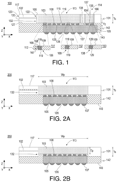
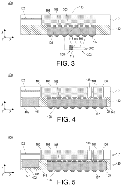
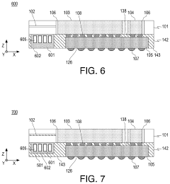
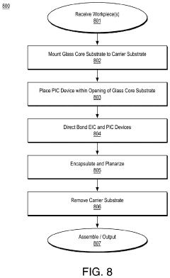
- The integration of photonic and electrical integrated circuit devices using direct die-to-die connections and hybrid bonding techniques within a glass core substrate, eliminating the need for solder bumping and enabling scalable packaging with reduced z-height and latency, while incorporating optical waveguides and cooling structures for enhanced performance.
Standardization Efforts
Standardization efforts in photodiode component compatibility for research setups have gained significant momentum in recent years. These initiatives aim to address the challenges of interoperability and reproducibility across different laboratories and experimental configurations.
One of the primary focuses of standardization has been the development of common interface protocols for photodiode components. Industry leaders and research institutions have collaborated to establish uniform communication standards, ensuring that photodiodes from various manufacturers can seamlessly integrate into diverse research setups. This effort has resulted in the creation of standardized connectors and signal formats, facilitating easier integration and reducing compatibility issues.
Another key area of standardization involves the establishment of calibration procedures and reference standards for photodiode performance. Regulatory bodies and metrology institutes have worked together to define standardized methods for characterizing photodiode sensitivity, spectral response, and linearity. These efforts have led to the creation of traceable calibration standards, enabling more accurate and comparable measurements across different research environments.
Standardization has also extended to the realm of data formats and reporting protocols for photodiode measurements. Researchers and industry experts have developed common data structures and file formats to facilitate the exchange of experimental results and enhance reproducibility. These standardized data formats have greatly improved the ability to share and compare results between different research groups and institutions.
Furthermore, efforts have been made to standardize the terminology and specifications used in describing photodiode components. This has resulted in the creation of comprehensive glossaries and standardized datasheets, ensuring clear communication and reducing ambiguity when discussing photodiode characteristics and performance metrics.
The development of standardized testing procedures for photodiode components has been another crucial aspect of these efforts. Industry consortia have established agreed-upon methodologies for evaluating key parameters such as responsivity, dark current, and noise characteristics. These standardized tests enable more reliable comparisons between different photodiode models and manufacturers, facilitating informed decision-making in research setup design.
Lastly, standardization initiatives have addressed the need for consistent documentation and traceability in photodiode component manufacturing and quality control. Guidelines have been established for documenting production processes, material specifications, and quality assurance procedures. This emphasis on standardized documentation enhances transparency and reliability in the photodiode supply chain, benefiting both manufacturers and end-users in research environments.
Integration Strategies
Integration strategies for advancing photodiode component compatibility in research setups are crucial for optimizing experimental outcomes and enhancing overall system performance. One key approach involves standardizing interface protocols to ensure seamless communication between photodiodes and other components. This standardization can be achieved through the development of universal adapters or the adoption of industry-wide connection standards, facilitating easier integration across diverse research environments.
Another important strategy is the implementation of modular design principles in research setups. By creating modular photodiode units with plug-and-play capabilities, researchers can easily swap components without disrupting the entire system. This approach not only increases flexibility but also reduces downtime during maintenance or upgrades, ultimately improving research efficiency.
Customization of photodiode housings and mounting systems is another vital integration strategy. Tailoring these elements to specific research requirements ensures optimal positioning and alignment within the setup. This may involve the use of adjustable mounts, precision stages, or custom-designed enclosures that accommodate various experimental conditions while maintaining the integrity of the photodiode's performance.
Software integration plays a significant role in enhancing photodiode compatibility. Developing robust drivers and software interfaces that support a wide range of photodiode models and specifications allows for seamless data acquisition and analysis. This software-centric approach can also facilitate real-time calibration, error correction, and data processing, further improving the accuracy and reliability of research results.
Thermal management strategies are essential for maintaining photodiode performance and longevity within research setups. Implementing effective cooling solutions, such as heat sinks or thermoelectric coolers, can help regulate operating temperatures and minimize thermal noise. This is particularly important in high-power or sensitive applications where temperature fluctuations can significantly impact measurement accuracy.
Electromagnetic compatibility (EMC) considerations are crucial when integrating photodiodes into complex research environments. Employing proper shielding techniques, grounding practices, and signal isolation methods can mitigate electromagnetic interference and ensure reliable photodiode operation. This may involve the use of specialized EMC-compliant enclosures or the implementation of advanced filtering techniques to maintain signal integrity.
Lastly, developing standardized calibration and characterization protocols for integrated photodiode systems is vital for ensuring consistency and comparability across different research setups. This includes establishing procedures for measuring key parameters such as responsivity, linearity, and spectral response under various operating conditions. By adopting these standardized methods, researchers can more easily validate and reproduce results, fostering collaboration and advancing the field as a whole.
Unlock deeper insights with Patsnap Eureka Quick Research — get a full tech report to explore trends and direct your research. Try now!
Generate Your Research Report Instantly with AI Agent
Supercharge your innovation with Patsnap Eureka AI Agent Platform!